SLVSGF5A May   2023  – December 2023 DRV8845

PRODUCTION DATA  

  1.   1
  2. Features
  3. Applications
  4. Description
  5. Device Comparison
  6. Pin Configuration and Functions
  7. Specifications
    1. 6.1 Absolute Maximum Ratings
    2. 6.2 ESD Ratings
    3. 6.3 Recommended Operating Conditions
    4. 6.4 Thermal Information
    5. 6.5 Electrical Characteristics
    6. 6.6 Typical Operating Characteristics
  8. Detailed Description
    1. 7.1 Overview
    2. 7.2 Functional Block Diagram
    3. 7.3 Feature Description
      1. 7.3.1 Motor Configurations
      2. 7.3.2 Stepper Control Logic
      3. 7.3.3 DC Motor Control
      4. 7.3.4 PWM Current Control
      5. 7.3.5 Current Regulation and Decay Mode
      6. 7.3.6 Blanking Time
      7. 7.3.7 Charge Pump
      8. 7.3.8 Logic-Level Pin Diagram
      9. 7.3.9 Protection Circuits
        1. 7.3.9.1 VM Undervoltage Lockout (UVLO)
        2. 7.3.9.2 VCP Undervoltage Lockout (CPUV)
        3. 7.3.9.3 Overcurrent Protection (OCP)
        4. 7.3.9.4 Thermal Shutdown (OTSD)
        5. 7.3.9.5 Fault Condition Summary
    4. 7.4 Device Functional Modes
      1. 7.4.1 Sleep Mode (nSLEEP = 0)
      2. 7.4.2 Operating Mode (nSLEEP = 1)
      3. 7.4.3 nSLEEP Reset Pulse
      4. 7.4.4 Functional Modes Summary
  9. Application and Implementation
    1. 8.1 Application Information
    2. 8.2 Application Schematics
    3. 8.3 Application Curves
  10. Layout
    1. 9.1 Layout Guidelines
    2. 9.2 Bulk Capacitance
  11. 10Revision History
  12. 11Mechanical, Packaging, and Orderable Information

Package Options

Mechanical Data (Package|Pins)
Thermal pad, mechanical data (Package|Pins)
Orderable Information

Logic-Level Pin Diagram

Figure 7-8 gives the input structure for logic-level pins PHASEx, I0x, I1x and nSLEEP.
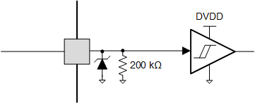
GUID-1ECA61DE-3EFF-46A3-9F8A-F79D710C97B8-low.gifFigure 7-8 Logic-level Input Pin Diagram