SLVSCY8B August 2015 – July 2016 DRV8870
PRODUCTION DATA.
- 1 Features
- 2 Applications
- 3 Description
- 4 Revision History
- 5 Pin Configuration and Functions
- 6 Specifications
- 7 Detailed Description
- 8 Application and Implementation
- 9 Power Supply Recommendations
- 10Layout
- 11Device and Documentation Support
- 12Mechanical, Packaging, and Orderable Information
Package Options
Refer to the PDF data sheet for device specific package drawings
Mechanical Data (Package|Pins)
- DDA|8
Thermal pad, mechanical data (Package|Pins)
- DDA|8
Orderable Information
7.3.1 Bridge Control
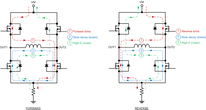
The DRV8870 output consists of four N-channel MOSFETs that are designed to drive high current. These outputs are controlled by the two logic inputs IN1 and IN2 as listed in Table 1.
Table 1. H-Bridge Control
| IN1 | IN2 | OUT1 | OUT2 | DESCRIPTION |
|---|---|---|---|---|
| 0 | 0 | High-Z | High-Z | Coast; H-bridge disabled to High-Z (sleep entered after 1 ms) |
| 0 | 1 | L | H | Reverse (Current OUT2 → OUT1) |
| 1 | 0 | H | L | Forward (Current OUT1 → OUT2) |
| 1 | 1 | L | L | Brake; low-side slow decay |
The inputs can be set to static voltages for 100% duty cycle drive, or they can be pulse-width modulated (PWM) for variable motor speed. When using PWM, switching between driving and braking typically works best. For example, to drive a motor forward with 50% of the maximum RPM, IN1 = 1 and IN2 = 0 during the driving period, and IN1 = 1 and IN2 = 1 during the other period. Alternatively, the coast mode (IN1 = 0, IN2 = 0) for fast current decay is also available. The input pins can be powered before VM is applied.
 Figure 4. H-Bridge Current Paths