SLVSCY8B August   2015  – July 2016 DRV8870

PRODUCTION DATA.  

  1. Features
  2. Applications
  3. Description
    1.     Device Images
      1.      Simplified Schematic
      2.      H-Bridge States
  4. Revision History
  5. Pin Configuration and Functions
    1.     Pin Functions
  6. Specifications
    1. 6.1 Absolute Maximum Ratings
    2. 6.2 ESD Ratings
    3. 6.3 Recommended Operating Conditions
    4. 6.4 Thermal Information
    5. 6.5 Electrical Characteristics
    6. 6.6 Typical Characteristics
  7. Detailed Description
    1. 7.1 Overview
    2. 7.2 Functional Block Diagram
    3. 7.3 Feature Description
      1. 7.3.1 Bridge Control
      2. 7.3.2 Sleep Mode
      3. 7.3.3 Current Regulation
      4. 7.3.4 Dead Time
      5. 7.3.5 Protection Circuits
        1. 7.3.5.1 VM Undervoltage Lockout (UVLO)
        2. 7.3.5.2 Overcurrent Protection (OCP)
        3. 7.3.5.3 Thermal Shutdown (TSD)
    4. 7.4 Device Functional Modes
      1. 7.4.1 PWM With Current Regulation
      2. 7.4.2 PWM Without Current Regulation
      3. 7.4.3 Static Inputs With Current Regulation
      4. 7.4.4 VM Control
  8. Application and Implementation
    1. 8.1 Application Information
    2. 8.2 Typical Application
      1. 8.2.1 Design Requirements
      2. 8.2.2 Detailed Design Procedure
        1. 8.2.2.1 Motor Voltage
        2. 8.2.2.2 Drive Current
        3. 8.2.2.3 Sense Resistor
      3. 8.2.3 Application Curves
  9. Power Supply Recommendations
    1. 9.1 Bulk Capacitance
  10. 10Layout
    1. 10.1 Layout Guidelines
    2. 10.2 Layout Example
    3. 10.3 Thermal Considerations
    4. 10.4 Power Dissipation
      1. 10.4.1 Heatsinking
  11. 11Device and Documentation Support
    1. 11.1 Documentation Support
      1. 11.1.1 Related Documentation
    2. 11.2 Receiving Notification of Documentation Updates
    3. 11.3 Community Resources
    4. 11.4 Trademarks
    5. 11.5 Electrostatic Discharge Caution
    6. 11.6 Glossary
  12. 12Mechanical, Packaging, and Orderable Information

Package Options

Refer to the PDF data sheet for device specific package drawings

Mechanical Data (Package|Pins)
  • DDA|8
Thermal pad, mechanical data (Package|Pins)
Orderable Information

Current Regulation

The DRV8870 device limits the output current based on the analog input, VREF, and the resistance of an external sense resistor on the ISEN pin according to Equation 1:

Equation 1. DRV8870 eq_I_trip_lvscy8.gif

For example, if VREF = 3.3 V and a RISEN = 0.15 Ω, the DRV8870 device limits motor current to 2.2 A no matter how much load torque is applied. For guidelines on selecting a sense resistor, see the Sense Resistor section.

When ITRIP is reached, the device enforces slow current decay by enabling both low-side FETs, and it does this for a time of tOFF (typically 25 µs).
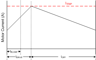
DRV8870 current_reg_lvscy8.gifFigure 5. Current-Regulation Time Periods

After tOFF elapses, the output is re-enabled according to the two inputs, INx. The drive time (tDRIVE) until reaching another ITRIP event heavily depends on the VM voltage, the back-EMF of the motor, and the inductance of the motor.