SLVSET1 August   2018 DRV8873

PRODUCTION DATA.  

  1. Features
  2. Applications
  3. Description
    1.     Simplified Schematic
  4. Revision History
  5. Pin Configuration and Functions
    1.     Pin Functions
  6. Specifications
    1. 6.1 Absolute Maximum Ratings
    2. 6.2 ESD Ratings
    3. 6.3 Recommended Operating Conditions
    4. 6.4 Thermal Information
    5. 6.5 Electrical Characteristics
    6. 6.6 SPI Timing Requirements
    7. 6.7 Typical Characteristics
  7. Detailed Description
    1. 7.1 Overview
    2. 7.2 Functional Block Diagram
    3. 7.3 Feature Description
      1. 7.3.1 Bridge Control
        1. 7.3.1.1 Control Modes
        2. 7.3.1.2 Half-Bridge Operation
        3. 7.3.1.3 Internal Current Sense and Current Regulation
        4. 7.3.1.4 Slew-Rate Control
        5. 7.3.1.5 Dead Time
        6. 7.3.1.6 Propagation Delay
        7. 7.3.1.7 nFAULT Pin
        8. 7.3.1.8 nSLEEP as SDO Reference
      2. 7.3.2 Motor Driver Protection Circuits
        1. 7.3.2.1 VM Undervoltage Lockout (UVLO)
        2. 7.3.2.2 VCP Undervoltage Lockout (CPUV)
        3. 7.3.2.3 Overcurrent Protection (OCP)
          1. 7.3.2.3.1 Latched Shutdown (OCP_MODE = 00b)
          2. 7.3.2.3.2 Automatic Retry (OCP_MODE = 01b)
          3. 7.3.2.3.3 Report Only (OCP_MODE = 10b)
          4. 7.3.2.3.4 Disabled (OCP_MODE = 11b)
        4. 7.3.2.4 Open-Load Detection (OLD)
          1. 7.3.2.4.1 Open-Load Detection in Passive Mode (OLP)
          2. 7.3.2.4.2 Open-Load Detection in Active Mode (OLA)
        5. 7.3.2.5 Thermal Shutdown (TSD)
          1. 7.3.2.5.1 Latched Shutdown (TSD_MODE = 0b)
          2. 7.3.2.5.2 Automatic Recovery (TSD_MODE = 1b)
        6. 7.3.2.6 Thermal Warning (OTW)
      3. 7.3.3 Hardware Interface
        1. 7.3.3.1 MODE (Tri-Level Input)
        2. 7.3.3.2 Slew Rate
    4. 7.4 Device Functional Modes
      1. 7.4.1 Motor Driver Functional Modes
        1. 7.4.1.1 Sleep Mode (nSLEEP = 0)
        2. 7.4.1.2 Disable Mode (nSLEEP = 1, DISABLE = 1)
        3. 7.4.1.3 Operating Mode (nSLEEP = 1, DISABLE = 0)
        4. 7.4.1.4 nSLEEP Reset Pulse
    5. 7.5 Programming
      1. 7.5.1 Serial Peripheral Interface (SPI) Communication
        1. 7.5.1.1 SPI Format
        2. 7.5.1.2 SPI for a Single Slave Device
        3. 7.5.1.3 SPI for Multiple Slave Devices in Parallel Configuration
        4. 7.5.1.4 SPI for Multiple Slave Devices in Daisy Chain Configuration
    6. 7.6 Register Maps
      1. 7.6.1 Status Registers
        1. 7.6.1.1 FAULT Status Register Name (address = 0x00)
          1. Table 21. FAULT Status Register Field Descriptions
        2. 7.6.1.2 DIAG Status Register Name (address = 0x01)
          1. Table 22. DIAG Status Register Field Descriptions
      2. 7.6.2 Control Registers
        1. 7.6.2.1 IC1 Control Register (address = 0x02)
          1. Table 24. IC1 Control Register Field Descriptions
        2. 7.6.2.2 IC2 Control Register (address = 0x03)
          1. Table 25. IC2 Control Register Field Descriptions
        3. 7.6.2.3 IC3 Control Register (address = 0x04)
          1. Table 26. IC3 Control Register Field Descriptions
        4. 7.6.2.4 IC4 Control Register (address = 0x05)
          1. Table 27. IC4 Control Register Field Descriptions
  8. Application and Implementation
    1. 8.1 Application Information
    2. 8.2 Typical Application
      1. 8.2.1 Design Requirements
        1. 8.2.1.1 Motor Voltage
        2. 8.2.1.2 Drive Current and Power Dissipation
        3. 8.2.1.3 Sense Resistor
      2. 8.2.2 Detailed Design Procedure
        1. 8.2.2.1 Thermal Considerations
        2. 8.2.2.2 Heatsinking
      3. 8.2.3 Application Curves
  9. Power Supply Recommendations
    1. 9.1 Bulk Capacitance Sizing
  10. 10Layout
    1. 10.1 Layout Guidelines
    2. 10.2 Layout Example
  11. 11Device and Documentation Support
    1. 11.1 Documentation Support
      1. 11.1.1 Related Documentation
    2. 11.2 Receiving Notification of Documentation Updates
    3. 11.3 Community Resources
    4. 11.4 Trademarks
    5. 11.5 Electrostatic Discharge Caution
    6. 11.6 Glossary
  12. 12Mechanical, Packaging, and Orderable Information
    1. 12.1 Package Option Addendum
      1. 12.1.1 Packaging Information
      2. 12.1.2 Tape and Reel Information

Package Options

Mechanical Data (Package|Pins)
Thermal pad, mechanical data (Package|Pins)
Orderable Information

Control Modes

The device output consists of four N-channel MOSFETs that are designed to drive high current. The MOSFETs are controlled by two logic inputs, EN/IN1 and PH/IN2, in three different input modes to support various commutation and control methods, as shown in the logic tables (Table 4, Table 5, and Table 6). In the Independent PWM mode, the fault handling is performed independently for each half bridge. For example, if an overcurrent condition (OCP) is detected in half-bridge 1, only the half-bridge 1 output (OUT1) is disabled and half-bridge 2 continues to operate based on the IN2 input.

Table 4. PH/EN Mode Truth Table

nSLEEP DISABLE EN/IN1 PH/IN2 OUT1 OUT2
0 X X X Hi-Z Hi-Z
1 1 X X Hi-Z Hi-Z
1 0 0 X H H
1 0 1 0 L H
1 0 1 1 H L

Table 5. PWM Mode Truth Table

nSLEEP DISABLE EN/IN1 PH/IN2 OUT1 OUT2
0 X X X Hi-Z Hi-Z
1 1 X X Hi-Z Hi-Z
1 0 0 0 Hi-Z Hi-Z
1 0 0 1 L H
1 0 1 0 H L
1 0 1 1 H H

Table 6. Independent Mode Truth Table

nSLEEP DISABLE EN/IN1 PH/IN2 OUT1 OUT2
0 X X X Hi-Z Hi-Z
1 1 X X Hi-Z Hi-Z
1 0 0 0 L L
1 0 0 1 L H
1 0 1 0 H L
1 0 1 1 H H

The inputs can be set to static voltages for 100% duty cycle drive, or they can be pulse-width modulated (PWM) for variable motor speed. When using PWM mode (MODE = 1), switching between driving and braking typically is best. For example, to drive a motor forward with 50% of its maximum revolutions per minute (RPM), the IN1 pin is high and the IN2 pin is low during the driving period. During the other period in this example, the IN1 pin is high and the IN2 pin is high.
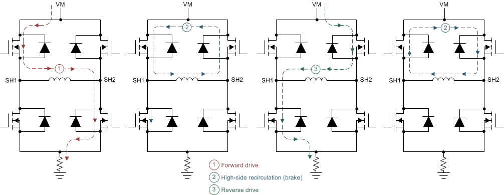
DRV8873 drv8873-q1-h-bridge-current-paths.gifFigure 10. Half-Bridge Current Paths

In the Independent PWM mode, to independently put the outputs of the half bridge in the high-impedance (Hi-Z) state, the OUT1_DIS or OUT2_DIS bit in the IC3 register must be set to 1b. Writing a logic 1 to the OUT1_DIS bit disables the OUT1 output. Writing a logic 1 to the OUT2_DIS bit disables the OUT2 output. The default value in these registers is 0b. The option to independently set the outputs of the half bridge in the Hi-Z state is not available for the hardware version of the device.