SNLS399B January 2012 – January 2015 DS100DF410
PRODUCTION DATA.
- 1 Features
- 2 Applications
- 3 Description
- 4 Revision History
- 5 Pin Configuration and Functions
- 6 Specifications
-
7 Detailed Description
- 7.1 Overview
- 7.2 Functional Block Diagram
- 7.3
Feature Description
- 7.3.1 Device Data Path Operation
- 7.3.2 Signal Detect
- 7.3.3 CTLE
- 7.3.4 DFE
- 7.3.5 Clock and Data Recovery
- 7.3.6 Output Driver
- 7.3.7 CTLE Boost Setting
- 7.3.8 DFE Tap Weight and Polarity Setting
- 7.3.9 Driver Output Voltage
- 7.3.10 Driver Output De-Emphasis
- 7.3.11 Driver Output Rise/Fall Time
- 7.3.12 Ref_mode 0 Mode (Reference Clock Not Required)
- 7.3.13 Ref_mode 3 Mode (Reference Clock Required)
- 7.3.14 False Lock Detector Setting
- 7.3.15 Reference Clock In
- 7.3.16 Reference Clock Out
- 7.3.17 Daisy Chain of REFCLK_OUT to REFCLK_IN
- 7.3.18 INT
- 7.3.19 LOCK_3, LOCK_2, LOCK_1, and LOCK_0
- 7.4 Device Functional Modes
- 7.5
Programming
- 7.5.1 SMBus Strap Observation
- 7.5.2 Device Revision and Device ID
- 7.5.3 Control/Shared Register Reset
- 7.5.4 Interrupt Channel Flag Bits
- 7.5.5 SMBus Master Mode Control Bits
- 7.5.6 Resetting Individual Channels of the Retimer
- 7.5.7 Interrupt Status
- 7.5.8 Overriding the CTLE Boost Setting
- 7.5.9 Overriding the VCO CAP DAC Values
- 7.5.10 Overriding the Output Multiplexer
- 7.5.11 Overriding the VCO Divider Selection
- 7.5.12 Using the PRBS Generator
- 7.5.13 Using the Internal Eye Opening Monitor
- 7.5.14 Overriding the DFE Tap Weights and Polarities
- 7.5.15 Enabling Slow Rise/Fall Time on the Output Driver
- 7.5.16 Inverting the Output Polarity
- 7.5.17 Overriding the Figure of Merit for Adaptation
- 7.5.18 Setting the Rate and Subrate for Lock Acquisition
- 7.5.19 Setting the Adaptation/Lock Mode
- 7.5.20 Initiating Adaptation
- 7.5.21 Setting the Reference Enable Mode
- 7.5.22 Overriding the CTLE Settings Used for CTLE Adaptation
- 7.5.23 Setting the Output Differential Voltage
- 7.5.24 Setting the Output De-emphasis Setting
- 7.6 Register Maps
- 8 Application and Implementation
- 9 Power Supply Recommendations
- 10Layout
- 11Device and Documentation Support
- 12Mechanical, Packaging, and Orderable Information
Package Options
Mechanical Data (Package|Pins)
- RHS|48
Thermal pad, mechanical data (Package|Pins)
- RHS|48
Orderable Information
6 Specifications
6.1 Absolute Maximum Ratings (1)
over operating free-air temperature range (unless otherwise noted)(1) Stresses beyond those listed under Absolute Maximum Ratings may cause permanent damage to the device. These are stress ratings only, which do not imply functional operation of the device at these or any other conditions beyond those indicated under Recommended Operating Conditions. Exposure to absolute-maximum-rated conditions for extended periods may affect device reliability.
6.2 ESD Ratings
| VALUE | UNIT | |||
|---|---|---|---|---|
| V(ESD) | ESD Rating | Human Body Model (HBM), per ANSI/ESDA/JEDEC JS-001, all pins(1) | ±6000 | V |
| Machine Model (MM), STD - JESD22-A115-A(3) | ±250 | |||
| Charged Device Model (CDM), per JEDEC specification JESD22-C101, all pins(2) | ±1250 | |||
(1) JEDEC document JEP155 states that 6000-V HBM allows safe manufacturing with a standard ESD control process.
(2) JEDEC document JEP157 states that 1250-V CDM allows safe manufacturing with a standard ESD control process.
(3) JEDEC document JEP157 states that 250-V MM allows safe manufacturing with a standard ESD control process.
6.3 Recommended Operating Conditions
over operating free-air temperature range (unless otherwise noted)| MIN | NOM | MAX | UNIT | |
|---|---|---|---|---|
| Supply Voltage (VDD to GND) | 2.375 | 2.5 | 2.625 | V |
| Ambient Temperature | -40 | 25 | +85 | °C |
6.4 Thermal Information(2)
| THERMAL METRIC(1) | DS100DF410 | UNIT | |
|---|---|---|---|
| WQFN | |||
| 48 PINS | |||
| RθJA | Junction-to-ambient thermal resistance | 26.1 | °C/W |
(1) For more information about traditional and new thermal metrics, see the IC Package Thermal Metrics application report, SPRA953.
(2) No airflow, 4-layer JEDEC, 9 thermal vias
6.5 Electrical Characteristics
Over recommended operating supply and temperature ranges with default register settings unless otherwise specified. (1)| PARAMETER | TEST CONDITIONS | MIN | TYP | MAX | UNIT | |
|---|---|---|---|---|---|---|
| POWER | ||||||
| PD | Power supply consumption | Average Power Consumption(2) | 720 | mW | ||
| Max Transient Power Supply Current (3) | 500 | 610 | mA | |||
| NTPS | Supply noise tolerance (4) | 50 Hz to 100 Hz | 100 | mVP-P | ||
| 100 Hz to 10 MHz | 40 | mVP-P | ||||
| 10 MHz to 5.0 GHz | 10 | mVP-P | ||||
| 2.5V LVCMOS DC SPECIFICATIONS | ||||||
| VIH | High level input voltage | 1.75 | VDD | V | ||
| High level (ADDR[3:0] pins) | 2.28 | VDD | V | |||
| VIL | Low level input voltage | GND | 0.7 | V | ||
| Low level input voltage (ADDR[3:0] pins) | GND | 0.335 | V | |||
| VOH | High level output voltage | IOH = -3mA | 2.0 | V | ||
| VOL | Low level output voltage | IOL = 3mA | 0.4 | V | ||
| IIN | Input leakage current | VIN = VDD | 10 | μA | ||
| VIN = GND | –10 | μA | ||||
| IIH | Input high current (EN_SMB pin) | VIN = VDD | 55 | μA | ||
| IIL | Input low current (EN_SMB pin) | VIN = GND | –110 | μA | ||
| 3.3 V LVCMOS DC SPECIFICATIONS (SDA, SDC, INT) | ||||||
| VIH | High level input voltage | VDD = 2.5 V | 1.75 | 3.6 | V | |
| VIL | Low level input voltage | VDD = 2.5 V | GND | 0.7 | V | |
| VOL | Low level output voltage | IPULLUP = 3mA | 0.4 | V | ||
| IIH | Input high current | VIN = 3.6 V, VDD = 2.5 V | 20 | 40 | μA | |
| IIL | Input low current | VIN = GND, VDD = 2.5 V | –10 | 10 | μA | |
| fSDC | SMBus clock rate | Slave Mode | 10 | 400 | kHz | |
| Master Mode(5) | 400 | kHz | ||||
| DATA BIT RATES | ||||||
| RB | Bit rate range | 10.3125 Gbps Ethernet | 10.1 | 10.6 | Gbps | |
| 1.25 Gbps Ethernet | 1.2 | 1.3 | Gbps | |||
| SIGNAL DETECT | ||||||
| SDH | Signal detect ON threshold level | Default differential input signal level to assert signal detect, 10.3125 Gbps, PRBS-31 |
70 | mVp-p | ||
| SDL | Signal detect OFF threshold level | Default differential input signal level to de-assert signal detect, 10.3125 Gbps, PRBS-31 |
10 | mVp-p | ||
| RECEIVER INPUTS (RXPn, RXNn) | ||||||
| VTX2, min | Minimum source transmit launch signal level (IN, diff) | See (5) | 600 | mVP-P | ||
| VTX2, max | 1000 | mVP-P | ||||
| VTX1, max | See (6) | 1200 | mVP-P | |||
| VTX0, max | See (7) | 1600 | mVP-P | |||
| LRI | Maximum differential input return loss - |SDD11| | 100 MHz – 6 GHz(8) | -15 | dB | ||
| ZD | Differential input impedance | 100 MHz – 6 GHz | 100 | Ω | ||
| ZS | Single-ended input impedance | 100 MHz – 6 GHz | 50 | Ω | ||
| DRIVER OUTPUTS (TXPn, TXNn) | ||||||
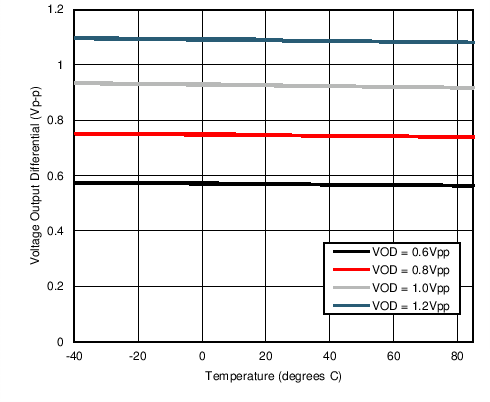
| VOD0 | Differential output voltage | Differential measurement with OUT+ and OUT- terminated by 50Ω to GND, AC-Coupled, SMBus register VOD control (Register 0x2d bits 2:0) set to 0, minimum VOD De-emphasis control set to minimum (0 dB) |
400 | 675 | mVP-P | |
| VOD7 | Differential output voltage | Differential measurement with OUT+ and OUT- terminated by 50Ω to GND, AC-Coupled SMBus register VOD control (Register 0x2d bits 2:0) set to 7, maximum VOD De-emphasis control set to minimum (0 dB) |
1000 | mVP-P | ||
| VOD_DE | De-emphasis level (10) | Differential measurement with OUT+ and OUT- terminated by 50Ω to GND, AC-Coupled Set by SMBus register control to maximum de-emphasis setting Relative to the nominal 0 dB de-emphasis level set at the minimum de-emphasis setting |
-12 | dB | ||
| tR, tF | Transition time (rise and fall times)(10)(11) | Transition time control = Full Slew Rate | 39 | ps | ||
| Transition time control = Limited Slew Rate | 50 | ps | ||||
| LRO | Maximum differential output return loss - |SDD22| | 100 MHz – 6 GHz (8) | –15 | dB | ||
| tDP | Propagation delay | Retimed data(9) | 300 | ps | ||
| TDE | De-emphasis pulse duration(12) | Measured at VOD = 1000 mVP-P, de-emphasis setting = -12 dB | 75 | ps | ||
| TJ | Output total jitter | Measured at BER = 10-12(13) | 10 | ps | ||
| TSKEW | Intra pair skew | Difference in 50% crossing between TXPn and TXNn for any output | 3 | ps | ||
| Channel-to-channel skew | 7 | ps | ||||
| CLOCK AND DATA RECOVERY | ||||||
| BWPLL | PLL Bandwidth, -3 dB | Measured at 10.3125 Gbps | 5 | MHz | ||
| JTOL | Input sinusoidal jitter tolerance 10 kHz to 250 MHz sinusoidal jitter frequency |
Measured at BER = 10-15 | 0.6 | UI | ||
| JTRANS | Jitter transfer sinusoidal jitter at 10 MHz jitter frequency | Measured at BER = 10-15 | -6 | dB | ||
| TLOCK | CDR Lock Time | Measured at 10.3125 Gbps | 15 | ms | ||
| RECOMMENDED REFERENCE CLOCK SPECS | ||||||
| REFf | Input reference clock frequency | 24.9975 | 25 | 25.0025 | MHz | |
| REFCLK_INPW | Minimum REFCLK_IN Pulse Width | At REFCLK_IN pin | 4 | ns | ||
| REFCLK_ OUTDCD |
REFCLK_OUT duty cycle distortion | CL = 5 pF | 0.55 | ns | ||
| REFVIH | Reference clock input min high threshold | 1.75 | V | |||
| REFVIL | Reference clock input max low threshold | 0.7 | V | |||
(1) Typical values represent most likely parametric norms at VDD = 2.5V, TA = 25°C, and at the Recommended Operation Conditions at the time of product characterization.
(2) VDD= 2.5V, TA = 25°C. All four channels active and locked. DFE powered-up and enabled.
(3) Maximum power supply current during lock acquisition. All four channels active, all four channels unlocked, all registers at default settings.
(4) Allowed supply noise (mVP-P sine wave) under typical conditions.
(5) EEPROM device used for Master mode programming must support fSDC greater than 400kHz.
(6) Differential signal amplitude at the transmitter output providing < 1x10-12 bit error rate. Measured at 10.3125 Gbps with a PRBS-31 data pattern. Input transmission channel is 40-inch long FR-4 stripline, 4-mil trace width.
(7) Differential signal amplitude at the transmitter output providing < 1x10-12 bit error rate. Measured at 10.3125 Gbps with a PRBS-31 data pattern. No input transmission channel.
(8) Measured with 10 MHz clock pattern output.
(9) Typical at 10.3125 Gbps bit rate.
(10) Measured with clock-like {11111 00000} pattern.
(11) Slew rate is controlled by SMBus register settings.
(12) De-emphasis pulse width varies with VOD and de-emphasis settings.
(13) Typical with no output de-emphasis, minimum output transmission channel.