SNLS461A May 2013 – June 2015 DS110DF111
PRODUCTION DATA.
- 1 Features
- 2 Applications
- 3 Description
- 4 Revision History
- 5 Pin Configuration and Functions
- 6 Specifications
-
7 Detailed Description
- 7.1 Overview
- 7.2 Functional Block Diagram
- 7.3 Feature Description
- 7.4 Device Functional Modes
- 7.5
Programming
- 7.5.1
SMBus Interface
- 7.5.1.1 Address Lines
- 7.5.1.2 Device Configuration in SMBus Slave Mode
- 7.5.1.3 Bit Fields in the Register Set
- 7.5.1.4 Writing to and Reading From the Control/Shared Registers
- 7.5.1.5 SMBus Strap Observation
- 7.5.1.6 Interrupt Channel Flag Bits
- 7.5.1.7 Control/Shared Register Reset
- 7.5.1.8 Device Revision and Device ID
- 7.5.1.9 Channel Select Register
- 7.5.1.10 Resetting Individual Channels of the Retimer
- 7.5.1.11 Rate and Subrate Setting
- 7.5.1.12 Overriding the CTLE Boost Setting
- 7.5.1.13 Overriding the Output Multiplexer
- 7.5.1.14 Overriding the VCO Divider Selection
- 7.5.1.15 Using the Internal Eye Opening Monitor
- 7.5.1.16 Overriding the DFE Tap Weights and Polarities
- 7.5.1.17 Enabling Slow Rise/Fall Time on the Output Driver
- 7.5.1.18 Using the PRBS Generator
- 7.5.1.19 Inverting the Output Polarity
- 7.5.1.20 Overriding the Figure of Merit Adaption
- 7.5.1.21 Setting the Rate and Subrate for Lock Acquisition
- 7.5.1.22 Setting the Adaption/Lock Mode
- 7.5.1.23 Initiating Adaption
- 7.5.1.24 Overriding the CTLE Settings used for CTLE Adaption
- 7.5.1.25 Setting the Output Differential Voltage
- 7.5.1.26 Setting the Output De-Emphasis Setting
- 7.5.1.27 CTLE Setting for Divide by 4 and Divide by 8 VCO Ranges
- 7.5.1
SMBus Interface
- 7.6 Register Maps
- 8 Applications and Implementation
- 9 Power Supply Recommendations
- 10Layout
- 11Device and Documentation Support
- 12Mechanical, Packaging, and Orderable Information
Package Options
Mechanical Data (Package|Pins)
- RTW|24
Thermal pad, mechanical data (Package|Pins)
- RTW|24
Orderable Information
9 Power Supply Recommendations
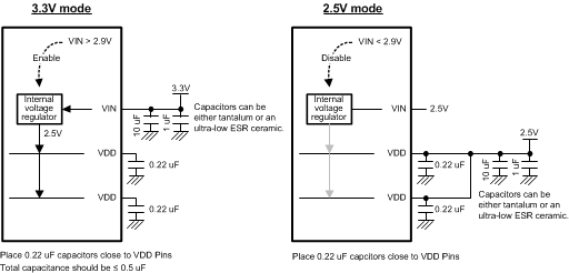
The DS110DF111 has an optional internal voltage regulator to provide the 2.5-V supply. In 3.3-V mode operation, the VIN pin = 3.3 V is used as the power supply input to the device. The internal regulator provides 2.5 V to the VDD pins of the device. A 0.22-uF cap is needed at each of the 2 VDD pins for power supply de-coupling (total capacitance should be ≤ 0.5 µF). These local decoupling capacitors should be the only connection to the DS110DF111 VDD net as the internal regulator is not designed to supply power to additional devices. In 2.5-V mode operation, the VIN pin should be connected to directly to the 2.5-V supply, a voltage less than 2.9 V will disable the internal regulator allowing an external supply to power the DS110DF111
 Figure 12. DS110DF111 Power Supply and Regulator Connections