SNLS430C October 2012 – August 2014 DS125BR111
PRODUCTION DATA.
- 1 Features
- 2 Applications
- 3 Description
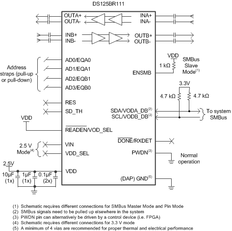
- 4 Simplified Schematic
- 5 Revision History
- 6 Pin Configuration and Functions
- 7 Specifications
- 8 Detailed Description
- 9 Application and Implementation
- 10Power Supply Recommendations
- 11Layout
- 12Device and Documentation Support
- 13Mechanical, Packaging, and Orderable Information
Package Options
Mechanical Data (Package|Pins)
- RTW|24
Thermal pad, mechanical data (Package|Pins)
- RTW|24
Orderable Information
1 Features
- Low 65 mW/Channel (typ) Power Consumption
- Supports Link Training
- Supports Out-of-Band (OOB) Signaling
- Advanced Signal Conditioning I/O
- Receive CTLE up to 10 dB at 6 GHz
- Linear Output Driver
- Output Voltage Range over 1200 mV
- Programmable via Pin Selection, EEPROM, or SMBus Interface
- Single Supply Voltage: 2.5 V or 3.3 V
- −40°C to 85°C Operating Temperature Range
- Flow-thru Pinout in 4 mm × 4 mm 24-pin Leadless WQFN Package
2 Applications
- SAS-1/2/3 and SATA-1/2/3
- PCI Express 1/2/3
- Other Proprietary Interfaces up to 12.5 Gbps
3 Description
The DS125BR111 is an extremely low power high performance repeater/redriver designed to support 1-lane carrying high speed interface up to 12.5 Gbps. The receiver's continuous time linear equalizer (CTLE) provides a boost of 3-10 dB at 6 GHz in each channel. When operating in SAS-3 or PCIe Gen-3 applications, the DS125BR111 preserves transmit signal characteristics allowing the host controller and the end point to negotiate transmit equalizer coefficients. Transparency to the link training protocol maximizes the flexibility of the physical placement of the device within the interconnect and improves overall channel performance.
The programmable settings can be applied easily via pins, software (SMBus or I2C), or loaded via an external EEPROM. In EEPROM mode, the configuration information is automatically loaded on power up, which eliminates the need for an external microprocessor or software driver.
Device Information(1)
| PART NUMBER | PACKAGE | BODY SIZE (NOM) |
|---|---|---|
| DS125BR111 | WQFN (24) | 4.00mm x 4.00mm |
- For all available packages, see the orderable addendum at the end of the datasheet.
4 Simplified Schematic