SNLS430C October 2012 – August 2014 DS125BR111
PRODUCTION DATA.
- 1 Features
- 2 Applications
- 3 Description
- 4 Simplified Schematic
- 5 Revision History
- 6 Pin Configuration and Functions
- 7 Specifications
- 8 Detailed Description
- 9 Application and Implementation
- 10Power Supply Recommendations
- 11Layout
- 12Device and Documentation Support
- 13Mechanical, Packaging, and Orderable Information
Package Options
Mechanical Data (Package|Pins)
- RTW|24
Thermal pad, mechanical data (Package|Pins)
- RTW|24
Orderable Information
11 Layout
11.1 Layout Guidelines
The DS125BR111 pinout promotes makes for easy high speed routing and layout. To optimize DS125BR111 performance refer to the following guidelines;
- Differential pairs going into or out of the DS125BR111 should have adequate pair - pair spacing to minimize crosstalk. Keep a 5x spacing ratio as shown on the Blue pairs in the layout example.
- Place local VIN and VDD capacitors as close as possible to the device supply pins to ensure a low inductance layout. Often the best location is directly under the DS125BR111 pins.
- Use return current via connections to link reference planes locally. This ensures a low inductance return current path when the differential signal changes layers.
- Open up the supply planes around differential vias to better match the trace impedance.
- Place GND vias around the DAP perimeter to ensure optimal electrical and thermal performance.
- Use 0201 body size coupling capacitors whenever possible, 0402 body size capacitors can also be used if they are placed closer to the Rx on the channel.
11.2 Layout Example
In most cases DS125BR111 layouts will fit neatly into a single or 1-lane application. The example layout shows how to "flip" one of the DS125BR111 channels to produce a 2-channel unidirectional layout.
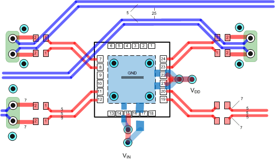 Figure 12. DS125BR111 Example Unidirectional Layout