SNLS430C October 2012 – August 2014 DS125BR111
PRODUCTION DATA.
- 1 Features
- 2 Applications
- 3 Description
- 4 Simplified Schematic
- 5 Revision History
- 6 Pin Configuration and Functions
- 7 Specifications
- 8 Detailed Description
- 9 Application and Implementation
- 10Power Supply Recommendations
- 11Layout
- 12Device and Documentation Support
- 13Mechanical, Packaging, and Orderable Information
Package Options
Mechanical Data (Package|Pins)
- RTW|24
Thermal pad, mechanical data (Package|Pins)
- RTW|24
Orderable Information
6 Pin Configuration and Functions
24 Pin
Package RTW
Top View
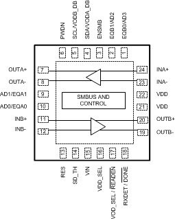
The center DAP on the package bottom is the only device GND connection. This pad must be connected to GND through multiple (minimum of 4) vias to ensure optimal electrical and thermal performance.
Pin Functions
| PIN | I/O | DESCRIPTION | |
|---|---|---|---|
| NAME | NO. | ||
| DIFFERENTIAL HIGH SPEED I/O | |||
| INB+, INB- | 11, 12 | I | Inverting and non-inverting CML differential inputs to the equalizer. On-chip 50 Ω termination resistor connects INB+ to VDD and INB- to VDD when enabled by RXDET control logic. AC coupling required on high-speed I/O |
| OUTB+, OUTB- | 20, 19 | O | Inverting and non-inverting 50 Ω driver outputs. Compatible with AC coupled CML inputs. AC coupling required on high-speed I/O |
| INA+, INA- | 24, 23 | I | Inverting and non-inverting CML differential inputs to the equalizer. On-chip 50 Ω termination resistor connects INA+ to VDD and INA- to VDD when enabled by RXDET control logic. AC coupling required on high-speed I/O |
| OUTA+, OUTA- | 7, 8 | O | Inverting and non-inverting 50 Ω driver outputs. Compatible with AC coupled CML inputs. AC coupling required on high-speed I/O |
| CONTROL PINS — SHARED (LVCMOS) | |||
| ENSMB | 3 | I, 4-LEVEL, LVCMOS |
System Management Bus (SMBus) enable Pin Tie 1 kΩ to VDD = Register Access SMBus Slave mode FLOAT = Read External EEPROM (Master SMBus Mode) Tie 1 kΩ to GND = Pin Mode |
| ENSMB = Float or 1 (SMBus MODEs) | |||
| SCL | 5 | I, LVCMOS, O, OPEN Drain |
ENSMB Master or Slave mode SMBus clock input Pin is enabled (slave mode). Clock output when loading EEPROM configuration (master mode). |
| SDA | 4 | I, LVCMOS, O, OPEN Drain |
ENSMB Master or Slave mode The SMBus bidirectional SDA Pin is enabled. Data input or open drain output. External pull-up required as per SMBus protocol (typically in the 2 kΩ to 5 kΩ range). This pin is 3.3 V-tolerant. |
| AD0-AD3 | 10, 9, 2, 1 | I, LVCMOS | ENSMB Master or Slave mode SMBus Slave Address Inputs. In SMBus mode, these Pins are the user set SMBus slave address inputs. |
| READEN | 17 | I, LVCMOS | ENSMB = Float: When using an External EEPROM, a logic low on this pin starts the load from the external EEPROM ENSMB = 1: When using SMBus Slave Mode the VOD_SEL/READEN pin must be tied Low for the AD[3:0] to be active. If this pin is tied High or Floated an address of 0xB0 will be used for the DS125BR111. |
| DONE | 18 | O, LVCMOS | When using an External EEPROM (ENSMB = Float), Valid Register Load Status Output HIGH = External EEPROM load failed or incomplete LOW = External EEPROM load passed |
| ENSMB = 0 (PIN MODE) | |||
| EQA0 EQB0 |
10 1 |
I, 4-LEVEL, LVCMOS |
EQA0 and EQB0 control the level of equalization of the A/B directions. The Pins are defined as EQx0 only when ENSMB is de-asserted (low). When ENSMB goes high the SMBus registers provide independent control of each channel. See Table 4. |
| EQA1 EQB1 |
9 2 |
I, 4-LEVEL, LVCMOS |
EQA1 and EQB1 are not used in the DS125BR111 design. These pins should always be tied to GND. |
| VODA_DB | 4 | I, 4-LEVEL, LVCMOS |
VODA_DB controls the CHA output amplitude dynamic range, for SAS and PCIe applications it should be held Low. The Pin is defined as VODA_DB only when ENSMB is de-asserted (low). When ENSMB goes high the SMBus registers provide control of each channel, pin 4 is converted to SDA. See Table 5. |
| VODB_DB | 5 | I, 4-LEVEL, LVCMOS |
VODB_DB controls the CHB output amplitude dynamic range, for SAS and PCIe applications it should be held Low. The Pin is defined as VODB_DB only when ENSMB is de-asserted (low). When ENSMB goes high the SMBus registers provide control of each channel, pin 5 is converted to SCL. See Table 5. |
| SD_TH | 14 | I, 4-LEVEL, LVCMOS |
Controls the internal Signal Detect Threshold. This detection threshold is for system debug only and does not control the high speed datapath. See Table 3. |
| VOD_SEL | 17 | I, 4-LEVEL, LVCMOS |
VOD_SEL controls the low frequency ratio of input voltage to output voltage amplitude. See Table 5. |
| RXDET | 18 | I, 4-LEVEL, LVCMOS |
The RXDET Pin controls the receiver detect function. Depending on the input level, a 50 Ω or > 50 kΩ termination to the power rail is enabled. In a SAS/SATA system RXDET should be set to a Logic "1" state to keep the termination always enabled. The RXDET pin only controls the RXDET function in PIN MODE. PCIe applications which require SMBus Mode functionality must utilize a specific register write sequence documented in PCIe Applications . If this sequence is not utilized, SMBus configuration modes will default the input terminations to active (50 Ω). See Table 2 . |
| CONTROL PINS — BOTH PIN AND SMBus MODES (LVCMOS) | |||
| RES | 13 | I, 4-LEVEL, LVCMOS |
Reserved: This input must be left Floating. |
| VDD_SEL | 16 | I, FLOAT | Controls the internal regulator Float = 2.5 V mode Tie GND = 3.3 V mode |
| PWDN | 6 | I, LVCMOS | Tie High = Low power - power down Tie GND = Normal Operation See Table 2. |
| POWER (See Figure 11) | |||
| VIN | 15 | Power | In 3.3 V mode, feed 3.3 V to VIN In 2.5 V mode, leave floating. |
| VDD | 21, 22 | Power | Power supply pins CML/analog 2.5 V mode, connect to 2.5 V 3.3 V mode, decouple each VDD pin with 0.22 µF cap to GND |
| GND | DAP | Power | Ground pad (DAP - die attach pad). |