SNLS491B July 2014 – February 2015 DS125BR820
PRODUCTION DATA.
- 1 Features
- 2 Applications
- 3 Description
- 4 Revision History
- 5 Pin Configuration and Functions
- 6 Specifications
- 7 Detailed Description
- 8 Applications and Implementation
- 9 Power Supply Recommendations
- 10Layout
- 11Device and Documentation Support
- 12Mechanical, Packaging, and Orderable Information
Package Options
Mechanical Data (Package|Pins)
- NJY|54
Thermal pad, mechanical data (Package|Pins)
Orderable Information
7 Detailed Description
7.1 Overview
The DS125BR820 provides linear equalization for lossy printed circuit board backplanes and balanced cables. The DS125BR820 operates in three modes: Pin Control Mode (ENSMB = 0), SMBus Slave Mode (ENSMB = 1) and SMBus Master Mode (ENSMB = Float) to load register information from external EEPROM.
7.2 Functional Block Diagram
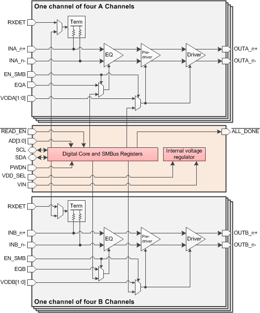
7.2.1 Functional Datapath Blocks
In an increasing number of high speed applications, transparency between Tx and Rx endpoints is essential to ensure high signal integrity. The DS125BR820 channel datapath uses one input gain stage equalization coupled with a linear driver. This combination provides a high level of transparency, thereby achieving greater drive distance in applications such as 40G-CR4, 40G-KR4, SAS, SATA, and PCIe that require Rx-Tx auto-negotiation and link-training. Refer to the Typical Applications section for more application information regarding recommended settings and placement.
7.3 Feature Description
The 4-level input pins use a resistor divider to help set the four valid control levels and provide a wider range of control settings when ENSMB = 0. There is an internal 30 kΩ pull-up and a 60 kΩ pull-down connected to the package pin. These resistors, together with the external resistor connection, combine to achieve the desired voltage level. By using the 1 kΩ pull-down, 20 kΩ pull-down, no connect, and 1 kΩ pull-up, the optimal voltage levels for each of the four input states are achieved as shown in Table 1.
Table 1. 4–Level Control Pin Settings
| RESULTING PIN VOLTAGE | |||
|---|---|---|---|
| LEVEL | SETTING | 3.3 V MODE | 2.5 V MODE |
| 0 | Tie 1 kΩ to GND | 0.10 V | 0.08 V |
| R | Tie 20 kΩ to GND | 1/3 x VIN | 1/3 x VDD |
| F | Float (leave pin open) | 2/3 x VIN | 2/3 x VDD |
| 1 | Tie 1 kΩ to VIN or VDD | VIN - 0.05 V | VDD - 0.04 V |
Typical 4-Level Input Thresholds
- Internal Threshold between 0 and R = 0.2 * VIN or VDD
- Internal Threshold between R and F = 0.5 * VIN or VDD
- Internal Threshold between F and 1 = 0.8 * VIN or VDD
In order to minimize the startup current associated with the integrated 2.5 V regulator, the 1 kΩ pull-up / pull-down resistors are recommended. If several four level inputs require the same setting, it is possible to combine two or more 1 kΩ resistors into a single lower value resistor. As an example, combining two inputs with a single 500 Ω resistor is a valid way to save board space.
7.4 Device Functional Modes
7.4.1 Pin Control Mode:
When in Pin Mode (ENSMB = 0), equalization and VOD (output amplitude) can be selected via pin control for both the A-channels and B-channels per Table 4. The RXDET pin provides either automatic or manual control for input termination (50 Ω or > 50 kΩ to VDD). The receiver electrical signal detect status threshold is adjustable via the SD_TH pin. By setting signal-detect threshold level via the SD_TH pin, status information about a valid signal detect assert/de-assert can be read back via SMBus registers. Pin control mode is ideal in situations where neither MCU or EEPROM is available to access the device via SMBus SDA/SCL lines.
7.4.2 Slave SMBus Mode:
When in Slave SMBus Mode (ENSMB = 1), the VOD (output amplitude), equalization, and termination disable features are all programmable on an individual channel basis, rather than in collective A-channel and B-channel groups. Upon assertion of ENSMB, the EQx and VODx settings are controlled by SMBus immediately. It is important to note that SMBus settings can only be changed from their defaults after asserting Register Enable by setting Reg 0x06[3] = 1. The EQx and VODx pins are subsequently converted to AD0-AD3 SMBus address inputs. The other external control pins (RXDET and SD_TH) remain active unless their respective registers are written to and the appropriate override bit is set. If the user overrides a pin control, the input voltage level of that control pin is ignored until ENSMB is driven low (Pin Mode). In the event that channels are powered down via the PWDN pin, the state of all register settings are not affected.
Table 2. Rx Detect Settings
| PWDN(1)
(Pin 52) |
RXDET (Pin 22) |
SMBus REG Bit[3:2] |
INPUT TERMINATION | RECOMMENDED USE | COMMENTS |
|---|---|---|---|---|---|
| 0 | 0 | 00 | Hi-Z | Manual Rx-Detect, input is Hi-Z | |
| 0 | R | 01 | Pre Detect: Hi-Z Post Detect: 50 Ω |
PCIe Only | Auto Rx-Detect, outputs test every 12 ms for 600 ms then stops; termination is Hi-Z until Rx detection; once detected input termination is 50 Ω Reset function by pulsing PWDN high for 5 µs then low again |
| 0 | F (Default) |
10 | Pre Detect: Hi-Z Post Detect: 50 Ω |
PCIe Only | Auto Rx-Detect, outputs test every 12 ms until detection occurs; termination is Hi-Z until Rx detection; once detected input termination is 50 Ω |
| 0 | 1 | 11 | 50 Ω | 40G-CR4/SR4/LR4 SAS/SATA |
Manual Rx-Detect, input is 50 Ω For 40G-CR4/SR4/LR4/SAS/SATA applications, it is required to use this setting. |
| 1 | X | X | Hi-Z | Power Down mode, input is Hi-Z, output drivers are disabled Used to reset Rx-Detect State Machine when held high for 5 µs |
Table 3. Signal Detect Status Threshold Level(1)(2)
| LEVEL | SD_TH (Pin 26) |
SMBus REG BIT[3:2] and[1:0] | [3:2] ASSERT LEVEL (mVp-p) | [1:0] DE-ASSERT LEVEL (mVp-p) | ||
|---|---|---|---|---|---|---|
| 3 Gbps | 12 Gbps | 3 Gbps | 12 Gbps | |||
| 1 | 0 | 10 | 18 | 75 | 14 | 55 |
| 2 | R | 01 | 12 | 40 | 8 | 22 |
| 3 | F (default) | 00 | 15 | 50 | 11 | 37 |
| 4 | 1 | 11 | 16 | 58 | 12 | 45 |
7.4.3 SMBus Master Mode
When in SMBus Master Mode (ENSMB = Float), the VOD (output amplitude), equalization, and termination disable features for multiple devices can be loaded via external EEPROM. By asserting a Float condition on the ENSMB pin, an external EEPROM writes register settings to each device in accordance with its SMBus slave address. The settings programmable by external EEPROM provide only a subset of all the register bits available via SMBus Slave Mode, and the bit-mapping between SMBus Slave Mode registers and Master SMBus registers can be referenced in Table 6. Once the EEPROM successfully finishes loading each device's register settings, the device reverts back to SMBus Slave Mode and releases SDA/SCL control to an external master MCU. If the EEPROM fails to load settings to a particular device, for example due to an invalid or blank hex file, a time-out occurs and the device hangs in an unknown state.
7.5 Signal Conditioning Settings
Equalization and VOD settings accessible via the pin controls are chosen to meet the needs of most high speed applications. These settings can also be controlled via the SMBus registers. Each pin input has a total of four possible voltage level settings. Table 4 and Table 5 show both the Pin Mode and SMBus Mode settings that are used in order to program the equalization and VOD gain for each DS125BR820 channel.
Table 4. Equalizer Settings(1)(2)
| EQUALIZATION BOOST RELATIVE to DC | |||||||
|---|---|---|---|---|---|---|---|
| LEVEL | EQA(3)
EQB |
EQ – 8 bits[7:0] | dB at 1.5 GHz |
dB at 2.5 GHz |
dB at 4 GHz |
dB at 5 GHz |
dB at 6 GHz |
| 1 | 0 | xxxx xx00 = 0x00 | 2.1 | 2.5 | 2.7 | 2.9 | 3.0 |
| 2 | R | xxxx xx01 = 0x01 | 4.0 | 5.1 | 6.4 | 6.8 | 7.4 |
| 3 | F | xxxx xx10 = 0x02 | 5.5 | 7.0 | 8.3 | 8.6 | 8.9 |
| 4 | 1 | xxxx xx11 = 0x03 | 6.8 | 8.3 | 9.5 | 9.6 | 9.8 |
Table 5. Output Voltage Settings(1)
| LEVEL | VODA1 VODB1 |
VODA0 VODB0 |
VOD - 3 bits[2:0] | VOD_DB - 3 bits[2:0] | VID Vp-p | VOD/VID Ratio(1) |
|---|---|---|---|---|---|---|
| -- | -- | -- | 000'b | 000'b | 1.2 | 0.57(2) |
| 1 | 0 | 0 | 001'b | 000'b | 1.2 | 0.65 |
| 2 | 0 | R | 010'b | 000'b | 1.2 | 0.71 |
| 3 | 0 | 1 | 011'b | 000'b | 1.2 | 0.77 |
| 4 | R | F | 100'b | 000'b | 1.2 | 0.83 |
| 5 | F | R | 101'b | 000'b | 1.2 | 0.90 |
| 6 | 1 | 0 | 110'b | 000'b | 1.2 | 1.00 |
| -- | -- | -- | 111'b | 000'b | 1.2 | 1.04(2)(3) |
7.6 Programming
The DS125BR820 device supports reading directly from an external EEPROM device by implementing SMBus Master Mode. When using SMBus Master Mode, the DS125BR820 reads directly from specific location in the external EEPROM. When designing a system for using the external EEPROM, the user must follow these specific guidelines.
- Maximum EEPROM size is 8K (1024 x 8-bit).
- Set ENSMB = Float — enable the SMBus Master Mode.
- The external EEPROM device address byte must be 0xA0 and capable of 1 MHz operation at 2.5 V and 3.3 V supply.
- Set the AD[3:0] inputs for SMBus address byte. When the AD[3:0] = 0000'b, the device address byte is 0xB0.
When tying multiple DS125BR820 devices to the SDA and SCL bus, use these guidelines to configure the devices:
- Use SMBus AD[3:0] address bits so that each device can load its configuration from the EEPROM. Example below is for four devices. The first device in the sequence is conventionally address 0xB0, while subsequent devices follow the address order listed below.
- U1: AD[3:0] = 0000 = 0xB0,
- U2: AD[3:0] = 0001 = 0xB2,
- U3: AD[3:0] = 0010 = 0xB4,
- U4: AD[3:0] = 0011 = 0xB6
- Use a pull-up resistor on SDA and SCL; value = 2 kΩ to 5 kΩ
- Daisy-chain READ_EN (Pin 26) and ALL_DONE (Pin 27) from one device to the next device in the sequence so that they do not compete for the EEPROM at the same time.
- Tie READ_EN of the first device in the chain (U1) to GND.
- Tie ALL_DONE of U1 to READ_EN of U2.
- Tie ALL_DONE of U2 to READ_EN of U3.
- Tie ALL_DONE of U3 to READ_EN of U4.
- Optional: Tie ALL_DONE output of U4 to a LED to show the devices have been loaded successfully.
Once the ALL_DONE status pin of the last device is flagged to indicate that all devices sharing the SMBus line have been successfully programmed, control of the SMBus line is released by the repeater and the device reverts back to SMBus Slave Mode. At this point, an external MCU can perform any additional Read or Write operations.
Below is an example of a 2 kbits (256 x 8-bit) EEPROM in hex format for the DS125BR820 device. The first three bytes of the EEPROM always contain a base header common and necessary to control initialization of all devices connected to the I2C bus. The CRC enable flag is used to enable or disable CRC checking. If CRC checking is disabled, a fixed pattern (8’hA5) is written/read instead of the CRC byte from the CRC location to simplify the control. There is a MAP bit to flag the presence of an address map that specifies the configuration data start address in the EEPROM. If the MAP bit is not present, the configuration data start address is assumed to follow the base header directly. Lastly, one bit in the base header is used to indicate whether EEPROM size > 256 bytes. This bit ensures that EEPROM slot addresses are formatted properly as one byte (EEPROM ≤ 256 bytes) or two bytes (EEPROM > 256 bytes) for subsequent address map headers. There are 37 bytes of data for each DS125BR820 device.
:2000000000001000000407002FAD4002FAD4002FAD4002FAD409805F5A8005F5A8005F5AD0
:200020008005F5A800005454000000000000000000000000000000000000000000000000F6
:20006000000000000000000000000000000000000000000000000000000000000000000080
:20008000000000000000000000000000000000000000000000000000000000000000000060
:2000A000000000000000000000000000000000000000000000000000000000000000000040
:2000C000000000000000000000000000000000000000000000000000000000000000000020
:2000E000000000000000000000000000000000000000000000000000000000000000000000
:200040000000000000000000000000000000000000000000000000000000000000000000A0
Note: The maximum EEPROM size supported is 8 kbits (1024 x 8 bits).
7.6.1 EEPROM Register Map for Single Device
A detailed EEPROM Register Map for a single device is shown in Table 6. For instances where multiple devices are written to EEPROM, the device starting address definitions align starting with Table 6 Byte 0x03.
Table 6. EEPROM Register Map - Single Device With Default Value
| EEPROM Address Byte | Bit 7 | Bit 6 | Bit 5 | Bit 4 | Bit 3 | Bit 2 | Bit 1 | Bit 0 | ||
|---|---|---|---|---|---|---|---|---|---|---|
| Description | 0x00 | CRC_EN | Address Map Present | EEPROM > 256 Bytes | Reserved | DEVICE COUNT[3] | DEVICE COUNT[2] | DEVICE COUNT[1] | DEVICE COUNT[0] | |
| Default Value | 0x00 | 0 | 0 | 0 | 0 | 0 | 0 | 0 | 0 | |
| Description | 0x01 | Reserved | Reserved | Reserved | Reserved | Reserved | Reserved | Reserved | Reserved | |
| Default Value | 0x00 | 0 | 0 | 0 | 0 | 0 | 0 | 0 | 0 | |
| Description | 0x02 | Max EEPROM Burst size[7] | Max EEPROM Burst size[6] | Max EEPROM Burst size[5] | Max EEPROM Burst size[4] | Max EEPROM Burst size[3] | Max EEPROM Burst size[2] | Max EEPROM Burst size[1] | Max EEPROM Burst size[0] | |
| Default Value | 0x00 | 0 | 0 | 0 | 0 | 0 | 0 | 0 | 0 | |
| Description | 0x03 | PWDN_CH7 | PWDN_CH6 | PWDN_CH5 | PWDN_CH4 | PWDN_CH3 | PWDN_CH2 | PWDN_CH1 | PWDN_CH0 | |
| SMBus Register | 0x01[7] | 0x01[6] | 0x01[5] | 0x01[4] | 0x01[3] | 0x01[2] | 0x01[1] | 0x01[0] | ||
| Default Value | 0x00 | 0 | 0 | 0 | 0 | 0 | 0 | 0 | 0 | |
| Description | 0x04 | Reserved | Reserved | Reserved | Reserved | Ovrd_PWDN | Reserved | Reserved | Reserved | |
| SMBus Register | 0x02[5] | 0x02[4] | 0x02[3] | 0x02[2] | 0x02[0] | 0x04[7] | 0x04[6] | 0x04[5] | ||
| Default Value | 0x00 | 0 | 0 | 0 | 0 | 0 | 0 | 0 | 0 | |
| Description | 0x05 | Reserved | Reserved | Reserved | Reserved | Reserved | Reserved | Ovrd_SD_TH | Reserved | |
| SMBus Register | 0x04[4] | 0x04[3] | 0x04[2] | 0x04[1] | 0x04[0] | 0x06[4] | 0x08[6] | 0x08[5] | ||
| Default Value | 0x04 | 0 | 0 | 0 | 0 | 0 | 1 | 0 | 0 | |
| Description | 0x06 | Reserved | Ovrd_RXDET | Reserved | Reserved | Reserved | Reserved | Reserved | Reserved | |
| SMBus Register | 0x08[4] | 0x08[3] | 0x08[2] | 0x08[1] | 0x08[0] | 0x0B[6] | 0x0B[5] | 0x0B[4] | ||
| Default Value | 0x07 | 0 | 0 | 0 | 0 | 0 | 1 | 1 | 1 | |
| Description | 0x07 | Reserved | Reserved | Reserved | Reserved | Reserved | Reserved | CH0_RXDET_1 | CH0_RXDET_0 | |
| SMBus Register | 0x0B[3] | 0x0B[2] | 0x0B[1] | 0x0B[0] | 0x0E[5] | 0x0E[4] | 0x0E[3] | 0x0E[2] | ||
| Default Value | 0x00 | 0 | 0 | 0 | 0 | 0 | 0 | 0 | 0 | |
| Description | 0x08 | Reserved | Reserved | Reserved | Reserved | Reserved | Reserved | CH0_EQ_1 | CH0_EQ_0 | |
| SMBus Register | 0x0F[7] | 0x0F[6] | 0x0F[5] | 0x0F[4] | 0x0F[3] | 0x0F[2] | 0x0F[1] | 0x0F[0] | ||
| Default Value | 0x2F | 0 | 0 | 1 | 0 | 1 | 1 | 1 | 1 | |
| Description | 0x09 | CH0_SCP | Reserved | Reserved | Reserved | Reserved | CH0_VOD_2 | CH0_VOD_1 | CH0_VOD_0 | |
| SMBus Register | 0x10[7] | 0x10[6] | 0x10[5] | 0x10[4] | 0x10[3] | 0x10[2] | 0x10[1] | 0x10[0] | ||
| Default Value | 0xAD | 1 | 0 | 1 | 0 | 1 | 1 | 0 | 1 | |
| Description | 0x0A | CH0_VOD_DB_2 | CH0_VOD_DB_1 | CH0_VOD_DB_0 | Reserved | CH0_THa_1 | CH0_THa_0 | CH0_THd_1 | CH0_THd_0 | |
| SMBus Register | 0x11[2] | 0x11[1] | 0x11[0] | 0x12[7] | 0x12[3] | 0x12[2] | 0x12[1] | 0x12[0] | ||
| Default Value | 0x40 | 0 | 1 | 0 | 0 | 0 | 0 | 0 | 0 | |
| Description | 0x0B | Reserved | Reserved | CH1_RXDET_1 | CH1_RXDET_0 | Reserved | Reserved | Reserved | Reserved | |
| SMBus Register | 0x15[5] | 0x15[4] | 0x15[3] | 0x15[2] | 0x16[7] | 0x16[6] | 0x16[5] | 0x16[4] | ||
| Default Value | 0x02 | 0 | 0 | 0 | 0 | 0 | 0 | 1 | 0 | |
| Description | 0x0C | Reserved | Reserved | CH1_EQ_1 | CH1_EQ_0 | CH1_SCP | Reserved | Reserved | Reserved | |
| SMBus Register | 0x16[3] | 0x16[2] | 0x16[1] | 0x16[0] | 0x17[7] | 0x17[6] | 0x17[5] | 0x17[4] | ||
| Default Value | 0xFA | 1 | 1 | 1 | 1 | 1 | 0 | 1 | 0 | |
| Description | 0x0D | Reserved | CH1_VOD_2 | CH1_VOD_1 | CH1_VOD_0 | CH1_VOD_DB_2 | CH1_VOD_DB_1 | CH1_VOD_DB_0 | Reserved | |
| SMBus Register | 0x17[3] | 0x17[2] | 0x17[1] | 0x17[0] | 0x18[2] | 0x18[1] | 0x18[0] | 0x19[7] | ||
| Default Value | 0xD4 | 1 | 1 | 0 | 1 | 0 | 1 | 0 | 0 | |
| Description | 0x0E | CH1_THa_1 | CH1_THa_0 | CH1_THd_1 | CH1_THd_0 | Reserved | Reserved | CH2_RXDET_1 | CH2_RXDET_0 | |
| SMBus Register | 0x19[3] | 0x19[2] | 0x19[1] | 0x19[0] | 0x1C[5] | 0x1C[4] | 0x1C[3] | 0x1C[2] | ||
| Default Value | 0x00 | 0 | 0 | 0 | 0 | 0 | 0 | 0 | 0 | |
| Description | 0x0F | Reserved | Reserved | Reserved | Reserved | Reserved | Reserved | CH2_EQ_1 | CH2_EQ_0 | |
| SMBus Register | 0x1D[7] | 0x1D[6] | 0x1D[5] | 0x1D[4] | 0x1D[3] | 0x1D[2] | 0x1D[1] | 0x1D[0] | ||
| Default Value | 0x2F | 0 | 0 | 1 | 0 | 1 | 1 | 1 | 1 | |
| Description | 0x10 | CH2_SCP | Reserved | Reserved | Reserved | Reserved | CH2_VOD_2 | CH2_VOD_1 | CH2_VOD_0 | |
| SMBus Register | 0x1E[7] | 0x1E[6] | 0x1E[5] | 0x1E[4] | 0x1E[3] | 0x1E[2] | 0x1E[1] | 0x1E[0] | ||
| Default Value | 0xAD | 1 | 0 | 1 | 0 | 1 | 1 | 0 | 1 | |
| Description | 0x11 | CH2_VOD_DB_2 | CH2_VOD_DB_1 | CH2_VOD_DB_0 | Reserved | CH2_THa_1 | CH2_THa_0 | CH2_THd_1 | CH2_THd_0 | |
| SMBus Register | 0x1F[2] | 0x1F[1] | 0x1F[0] | 0x20[7] | 0x20[3] | 0x20[2] | 0x20[1] | 0x20[0] | ||
| Default Value | 0x40 | 0 | 1 | 0 | 0 | 0 | 0 | 0 | 0 | |
| Description | 0x12 | Reserved | Reserved | CH3_RXDET_1 | CH3_RXDET_0 | Reserved | Reserved | Reserved | Reserved | |
| SMBus Register | 0x23[5] | 0x23[4] | 0x23[3] | 0x23[2] | 0x24[7] | 0x24[6] | 0x24[5] | 0x24[4] | ||
| Default Value | 0x02 | 0 | 0 | 0 | 0 | 0 | 0 | 1 | 0 | |
| Description | 0x13 | Reserved | Reserved | CH3_EQ_1 | CH3_EQ_0 | CH3_SCP | Reserved | Reserved | Reserved | |
| SMBus Register | 0x24[3] | 0x24[2] | 0x24[1] | 0x24[0] | 0x25[7] | 0x25[6] | 0x25[5] | 0x25[4] | ||
| Default Value | 0xFA | 1 | 1 | 1 | 1 | 1 | 0 | 1 | 0 | |
| Description | 0x14 | Reserved | CH3_VOD_2 | CH3_VOD_1 | CH3_VOD_0 | CH3_VOD_DB_2 | CH3_VOD_DB_1 | CH3_VOD_DB_0 | Reserved | |
| SMBus Register | 0x25[3] | 0x25[2] | 0x25[1] | 0x25[0] | 0x26[2] | 0x26[1] | 0x26[0] | 0x27[7] | ||
| Default Value | 0xD4 | 1 | 1 | 0 | 1 | 0 | 1 | 0 | 0 | |
| Description | 0x15 | CH3_THa_1 | CH3_THa_0 | CH3_THd_1 | CH3_THd_0 | Reserved | hi_idle_SD CH0-3 | hi_idle_SD CH4-7 | fast_SD CH0-3 | |
| SMBus Register | 0x27[3] | 0x27[2] | 0x27[1] | 0x27[0] | 0x28[6] | 0x28[5] | 0x28[4] | 0x28[3] | ||
| Default Value | 0x09 | 0 | 0 | 0 | 0 | 1 | 0 | 0 | 1 | |
| Description | 0x16 | fast_SD CH4-7 | lo_gain_SD CH0-3 | lo_gain_SD CH4-7 | Reserved | Reserved | CH4_RXDET_1 | CH4_RXDET_0 | Reserved | |
| SMBus Register | 0x28[2] | 0x28[1] | 0x28[0] | 0x2B[5] | 0x2B[4] | 0x2B[3] | 0x2B[2] | 0x2C[7] | ||
| Default Value | 0x80 | 1 | 0 | 0 | 0 | 0 | 0 | 0 | 0 | |
| Description | 0x17 | Reserved | Reserved | Reserved | Reserved | Reserved | CH4_EQ_1 | CH4_EQ_0 | CH4_SCP | |
| SMBus Register | 0x2C[6] | 0x2C[5] | 0x2C[4] | 0x2C[3] | 0x2C[2] | 0x2C[1] | 0x2C[0] | 0x2D[7] | ||
| Default Value | 0x5F | 0 | 1 | 0 | 1 | 1 | 1 | 1 | 1 | |
| Description | 0x18 | Reserved | Reserved | Reserved | Reserved | CH4_VOD_2 | CH4_VOD_1 | CH4_VOD_0 | CH4_VOD_DB_2 | |
| SMBus Register | 0x2D[6] | 0x2D[5] | 0x2D[4] | 0x2D[3] | 0x2D[2] | 0x2D[1] | 0x2D[0] | 0x2E[2] | ||
| Default Value | 0x5A | 0 | 1 | 0 | 1 | 1 | 0 | 1 | 0 | |
| Description | 0x19 | CH4_VOD_DB_1 | CH4_VOD_DB_0 | Reserved | CH4_THa_1 | CH4_THa_0 | CH4_THd_1 | CH4_THd_0 | Reserved | |
| SMBus Register | 0x2E[1] | 0x2E[0] | 0x2F[7] | 0x2F[3] | 0x2F[2] | 0x2F[1] | 0x2F[0] | 0x32[5] | ||
| Default Value | 0x80 | 1 | 0 | 0 | 0 | 0 | 0 | 0 | 0 | |
| Description | 0x1A | Reserved | CH5_RXDET_1 | CH5_RXDET_0 | Reserved | Reserved | Reserved | Reserved | Reserved | |
| SMBus Register | 0x32[4] | 0x32[3] | 0x32[2] | 0x33[7] | 0x33[6] | 0x33[5] | 0x33[4] | 0x33[3] | ||
| Default Value | 0x05 | 0 | 0 | 0 | 0 | 0 | 1 | 0 | 1 | |
| Description | 0x1B | Reserved | CH5_EQ_1 | CH5_EQ_0 | CH5_SCP | Reserved | Reserved | Reserved | Reserved | |
| SMBus Register | 0x33[2] | 0x33[1] | 0x33[0] | 0x34[7] | 0x34[6] | 0x34[5] | 0x34[4] | 0x34[3] | ||
| Default Value | 0xF5 | 1 | 1 | 1 | 1 | 0 | 1 | 0 | 1 | |
| Description | 0x1C | CH5_VOD_2 | CH5_VOD_1 | CH5_VOD_0 | CH5_VOD_DB_2 | CH5_VOD_DB_1 | CH5_VOD_DB_0 | Reserved | CH5_THa_1 | |
| SMBus Register | 0x34[2] | 0x34[1] | 0x34[0] | 0x35[2] | 0x35[1] | 0x35[0] | 0x36[7] | 0x36[3] | ||
| Default Value | 0xA8 | 1 | 0 | 1 | 0 | 1 | 0 | 0 | 0 | |
| Description | 0x1D | CH5_THa_0 | CH5_THd_1 | CH5_THd_0 | Reserved | Reserved | CH6_RXDET_1 | CH6_RXDET_0 | Reserved | |
| SMBus Register | 0x36[2] | 0x36[1] | 0x36[0] | 0x39[5] | 0x39[4] | 0x39[3] | 0x39[2] | 0x3A[7] | ||
| Default Value | 0x00 | 0 | 0 | 0 | 0 | 0 | 0 | 0 | 0 | |
| Description | 0x1E | Reserved | Reserved | Reserved | Reserved | Reserved | CH6_EQ_1 | CH6_EQ_0 | CH6_SCP | |
| SMBus Register | 0x3A[6] | 0x3A[5] | 0x3A[4] | 0x3A[3] | 0x3A[2] | 0x3A[1] | 0x3A[0] | 0x3B[7] | ||
| Default Value | 0x5F | 0 | 1 | 0 | 1 | 1 | 1 | 1 | 1 | |
| Description | 0x1F | Reserved | Reserved | Reserved | Reserved | CH6_VOD_2 | CH6_VOD_1 | CH6_VOD_0 | CH6_VOD_DB_2 | |
| SMBus Register | 0x3B[6] | 0x3B[5] | 0x3B[4] | 0x3B[3] | 0x3B[2] | 0x3B[1] | 0x3B[0] | 0x3C[2] | ||
| Default Value | 0x5A | 0 | 1 | 0 | 1 | 1 | 0 | 1 | 0 | |
| Description | 0x20 | CH6_VOD_DB_1 | CH6_VOD_DB_0 | Reserved | CH6_THa_1 | CH6_THa_0 | CH6_THd_1 | CH6_THd_0 | Reserved | |
| SMBus Register | 0x3C[1] | 0x3C[0] | 0x3D[7] | 0x3D[3] | 0x3D[2] | 0x3D[1] | 0x3D[0] | 0x40[5] | ||
| Default Value | 0x80 | 1 | 0 | 0 | 0 | 0 | 0 | 0 | 0 | |
| Description | 0x21 | Reserved | CH7_RXDET_1 | CH7_RXDET_0 | Reserved | Reserved | Reserved | Reserved | Reserved | |
| SMBus Register | 0x40[4] | 0x40[3] | 0x40[2] | 0x41[7] | 0x41[6] | 0x41[5] | 0x41[4] | 0x41[3] | ||
| Default Value | 0x05 | 0 | 0 | 0 | 0 | 0 | 1 | 0 | 1 | |
| Description | 0x22 | Reserved | CH7_EQ_1 | CH7_EQ_0 | CH7_SCP | Reserved | Reserved | Reserved | Reserved | |
| SMBus Register | 0x41[2] | 0x41[1] | 0x41[0] | 0x42[7] | 0x42[6] | 0x42[5] | 0x42[4] | 0x42[3] | ||
| Default Value | 0xF5 | 1 | 1 | 1 | 1 | 0 | 1 | 0 | 1 | |
| Description | 0x23 | CH7_VOD_2 | CH7_VOD_1 | CH7_VOD_0 | CH7_VOD_DB_2 | CH7_VOD_DB_1 | CH7_VOD_DB_0 | Reserved | CH7_THa_1 | |
| SMBus Register | 0x42[2] | 0x42[1] | 0x42[0] | 0x43[2] | 0x43[1] | 0x43[0] | 0x44[7] | 0x44[3] | ||
| Default Value | 0xA8 | 1 | 0 | 1 | 0 | 1 | 0 | 0 | 0 | |
| Description | 0x24 | CH7_THa_0 | CH7_THd_1 | CH7_THd_0 | Reserved | Reserved | Reserved | Reserved | Reserved | |
| SMBus Register | 0x44[2] | 0x44[1] | 0x44[0] | 0x47[3] | 0x47[2] | 0x47[1] | 0x47[0] | 0x48[7] | ||
| Default Value | 0x00 | 0 | 0 | 0 | 0 | 0 | 0 | 0 | 0 | |
| Description | 0x25 | Reserved | Reserved | Reserved | Reserved | Reserved | Reserved | Reserved | Reserved | |
| SMBus Register | 0x48[6] | 0x4C[7] | 0x4C[6] | 0x4C[5] | 0x4C[4] | 0x4C[3] | 0x4C[0] | 0x59[0] | ||
| Default Value | 0x00 | 0 | 0 | 0 | 0 | 0 | 0 | 0 | 0 | |
| Description | 0x26 | Reserved | Reserved | Reserved | Reserved | Reserved | Reserved | Reserved | Reserved | |
| SMBus Register | 0x5A[7] | 0x5A[6] | 0x5A[5] | 0x5A[4] | 0x5A[3] | 0x5A[2] | 0x5A[1] | 0x5A[0] | ||
| Default Value | 0x54 | 0 | 1 | 0 | 1 | 0 | 1 | 0 | 0 | |
| Description | 0x27 | Reserved | Reserved | Reserved | Reserved | Reserved | Reserved | Reserved | Reserved | |
| SMBus Register | 0x5B[7] | 0x5B[6] | 0x5B[5] | 0x5B[4] | 0x5B[3] | 0x5B[2] | 0x5B[1] | 0x5B[0] | ||
| Default Value | 0x54 | 0 | 1 | 0 | 1 | 0 | 1 | 0 | 0 | |
Table 7. Example Of EEPROM for Four Devices Using Two Address Maps
| EEPROM ADDRESS |
ADDRESS (Hex) |
EEPROM DATA |
COMMENTS |
|---|---|---|---|
| 0 | 00 | 0x43 | CRC_EN = 0, Address Map = 1, >256 bytes = 0, Device Count[3:0] = 3 |
| 1 | 01 | 0x00 | |
| 2 | 02 | 0x10 | EEPROM Burst Size |
| 3 | 03 | 0x00 | CRC not used |
| 4 | 04 | 0x0B | Device 0 Address Location |
| 5 | 05 | 0x00 | CRC not used |
| 6 | 06 | 0x0B | Device 1 Address Location |
| 7 | 07 | 0x00 | CRC not used |
| 8 | 08 | 0x30 | Device 2 Address Location |
| 9 | 09 | 0x00 | CRC not used |
| 10 | 0A | 0x30 | Device 3 Address Location |
| 11 | 0B | 0x00 | Begin Device 0, 1 - Address Offset 3 |
| 12 | 0C | 0x00 | |
| 13 | 0D | 0x04 | |
| 14 | 0E | 0x07 | |
| 15 | 0F | 0x00 | |
| 16 | 10 | 0x01 | EQ CHB0 = 0x01 |
| 17 | 11 | 0xAD | VOD CHB0 = 101'b |
| 18 | 12 | 0x00 | VOD_DB CHB0 = 000'b |
| 19 | 13 | 0x00 | |
| 20 | 14 | 0x1A | EQ CHB1 = 0x01 |
| 21 | 15 | 0xD0 | VOD CHB1 = 101'b, VOD_DB CHB1 = 000'b |
| 22 | 16 | 0x00 | |
| 23 | 17 | 0x01 | EQ CHB2 = 0x01 |
| 24 | 18 | 0xAD | VOD CHB2 = 101'b |
| 25 | 19 | 0x00 | VOD_DB CHB2 = 000'b |
| 26 | 1A | 0x00 | |
| 27 | 1B | 0x1A | EQ CHB3 = 0x01 |
| 28 | 1C | 0xD0 | VOD CHB3 = 101'b, VOD_DB CHB3 = 000'b |
| 29 | 1D | 0x09 | Signal Detect Status Threshold Control |
| 30 | 1E | 0x80 | Signal Detect Status Threshold Control |
| 31 | 1F | 0x07 | EQ CHA0 = 0x03 |
| 32 | 20 | 0x5C | VOD CHA0 = 110'b |
| 33 | 21 | 0x00 | VOD_DB CHA0 = 000'b |
| 34 | 22 | 0x00 | |
| 35 | 23 | 0x15 | EQ CHA1 = 0x00 |
| 36 | 24 | 0xC0 | VOD CHA1 = 110'b, VOD_DB CHA1 = 000'b |
| 37 | 25 | 0x00 | |
| 38 | 26 | 0x07 | EQ CHA2 = 0x03 |
| 39 | 27 | 0x5C | VOD CHA2 = 110'b |
| 40 | 28 | 0x00 | VOD_DB CHA2 = 000'b |
| 41 | 29 | 0x00 | |
| 42 | 2A | 0x75 | EQ CHA3 = 0x00 |
| 43 | 2B | 0xC0 | VOD CHA3 = 110'b, VOD_DB CHA3 = 000'b |
| 44 | 2C | 0x00 | |
| 45 | 2D | 0x00 | |
| 46 | 2E | 0x54 | |
| 47 | 2F | 0x54 | End Device 0, 1 - Address Offset 39 |
| 48 | 30 | 0x00 | Begin Device 2, 3 - Address Offset 3 |
| 49 | 31 | 0x00 | |
| 50 | 32 | 0x04 | |
| 51 | 33 | 0x07 | |
| 52 | 34 | 0x00 | |
| 53 | 35 | 0x01 | EQ CHB0 = 0x01 |
| 54 | 36 | 0xAB | VOD CHB0 = 011'b |
| 55 | 37 | 0x00 | VOD_DB CHB0 = 000'b |
| 56 | 38 | 0x00 | |
| 57 | 39 | 0x1A | EQ CHB1 = 0x01 |
| 58 | 3A | 0xB0 | VOD CHB1 = 011'b, VOD_DB CHB1 = 000'b |
| 59 | 3B | 0x00 | |
| 60 | 3C | 0x01 | EQ CHB2 = 0x01 |
| 61 | 3D | 0xAB | VOD CHB2 = 011'b |
| 62 | 3E | 0x00 | VOD_DB CHB2 = 000'b |
| 63 | 3F | 0x00 | |
| 64 | 40 | 0x1A | EQ CHB3 = 0x01 |
| 65 | 41 | 0xB0 | VOD CHB3 = 011'b, VOD_DB CHB3 = 000'b |
| 66 | 42 | 0x09 | Signal Detect Status Threshold Control |
| 67 | 43 | 0x80 | Signal Detect Status Threshold Control |
| 68 | 44 | 0x07 | EQ CHA0 = 0x03 |
| 69 | 45 | 0x5C | VOD CHA0 = 110'b |
| 70 | 46 | 0x00 | VOD_DB CHA0 = 000'b |
| 71 | 47 | 0x00 | |
| 72 | 48 | 0x15 | EQ CHA1 = 0x00 |
| 73 | 49 | 0xA0 | VOD CHA1 = 101'b, VOD_DB CHA1 = 000'b |
| 74 | 4A | 0x00 | |
| 75 | 4B | 0x07 | EQ CHA2 = 0x03 |
| 76 | 4C | 0x5C | VOD CHA2 = 110'b |
| 77 | 4D | 0x00 | VOD_DB CHA2 = 000'b |
| 78 | 4E | 0x00 | |
| 79 | 4F | 0x15 | EQ CHA3 = 0x00 |
| 80 | 50 | 0xA0 | VOD CHA3 = 101'b, VOD_DB CHA3 = 000'b |
| 81 | 51 | 0x00 | |
| 82 | 52 | 0x00 | |
| 83 | 53 | 0x54 | |
| 84 | 54 | 0x54 | End Device 2, 3 - Address Offset 39 |
Note: CRC_EN = 0, Address Map = 1, >256 byte = 0, Device Count[3:0] = 3. Multiple devices can point to the same address map. Maximum EEPROM size is 8 kbits (1024 x 8-bits).
7.7 Register Maps
The System Management Bus interface is compatible to SMBus 2.0 physical layer specification. Tie ENSMB = 1 kΩ to VDD (2.5 V mode) or VIN (3.3 V mode) to enable SMBus Slave Mode and allow access to the configuration registers.
The DS125BR820 uses AD[3:0] inputs in both SMBus Modes. These AD[3:0] pins are the user set SMBus slave address inputs and have internal pull-downs. Based on the SMBus 2.0 specification, the DS125BR820 has a 7-bit slave address. The LSB is set to 0'b (for a WRITE). When AD[3:0] pins are left floating or pulled low, AD[3:0] = 0000'b, and the device default address byte is 0xB0. The device supports up to 16 address bytes, as shown in Table 8:
Table 8. Device Slave Address Bytes
| AD[3:0] SETTINGS | FULL SLAVE ADDRESS BYTE (7-Bit ADDRESS + WRITE BIT) |
7-Bit SLAVE ADDRESS (HEX) |
|---|---|---|
| 0000 | B0 | 58 |
| 0001 | B2 | 59 |
| 0010 | B4 | 5A |
| 0011 | B6 | 5B |
| 0100 | B8 | 5C |
| 0101 | BA | 5D |
| 0110 | BC | 5E |
| 0111 | BE | 5F |
| 1000 | C0 | 60 |
| 1001 | C2 | 61 |
| 1010 | C4 | 62 |
| 1011 | C6 | 63 |
| 1100 | C8 | 64 |
| 1101 | CA | 65 |
| 1110 | CC | 66 |
| 1111 | CE | 67 |
The SDA/SCL pins are 3.3 V tolerant, but are not 5V tolerant. An external pull-up resistor is required on the SDA line. The resistor value can be from 2 kΩ to 5 kΩ depending on the voltage, loading and speed. The SCL may also require an external pull-up resistor and it depends on the Host that drives the bus.
7.7.1 Transfer Of Data Via The SMBus
During normal operation, the data on SDA must be stable during the time when SCL is High.
There are three unique states for the SMBus:
START: A High-to-Low transition on SDA while SCL is High indicates a message START condition.
STOP: A Low-to-High transition on SDA while SCL is High indicates a message STOP condition.
IDLE: If SCL and SDA are both High for a time exceeding tBUF from the last detected STOP condition or if they are High for a total exceeding the maximum specification for tHIGH, then the bus transfers to the IDLE state.
7.7.2 SMBus Transactions
The device supports WRITE and READ transactions. See Table 9 for register address, type (Read/Write, Read Only), default value, and function information.
7.7.3 Writing a Register
To write a register, the following protocol is used (see SMBus 2.0 specification).
- The Host drives a START condition, the 7-bit SMBus address, and a “0” indicating a WRITE.
- The Device (Slave) drives the ACK bit (“0”).
- The Host drives the 8-bit Register Address.
- The Device drives an ACK bit (“0”).
- The Host drive the 8-bit data byte.
- The Device drives an ACK bit (“0”).
- The Host drives a STOP condition.
The WRITE transaction is completed, the bus goes IDLE, and communication with other SMBus devices may now occur.
7.7.4 Reading a Register
To read a register, the following protocol is used (see SMBus 2.0 specification).
- The Host drives a START condition, the 7-bit SMBus address, and a “0” indicating a WRITE.
- The Device (Slave) drives the ACK bit (“0”).
- The Host drives the 8-bit Register Address.
- The Device drives an ACK bit (“0”).
- The Host drives a START condition.
- The Host drives the 7-bit SMBus Address, and a “1” indicating a READ.
- The Device drives an ACK bit “0”.
- The Device drives the 8-bit data value (register contents).
- The Host drives a NACK bit “1”indicating end of the READ transfer.
- The Host drives a STOP condition.
The READ transaction is completed, the bus goes IDLE, and communication with other SMBus devices may now occur.
7.7.5 Detailed Register Map
Table 9. SMBus Slave Mode Register Map
| Address | Register Name |
Bit | Field | Type | Default | EEPROM Reg Bit |
Description |
|---|---|---|---|---|---|---|---|
| 0x00 | Observation | 7 | Reserved | R/W | 0x00 | Set bit to 0 | |
| 6:3 | Address Bit AD[3:0] |
R | Observation of AD[3:0] bits [6]: AD3 [5]: AD2 [4]: AD1 [3]: AD0 |
||||
| 2 | EEPROM Read Done | R | 1 = Device completed the read from external EEPROM | ||||
| 1 | Reserved | R/W | Set bit to 0 | ||||
| 0 | Reserved | R/W | Set bit to 0 | ||||
| 0x01 | PWDN Channels | 7:0 | PWDN CHx | R/W | 0x00 | Yes | Power Down per Channel [7]: CH7 – CHA_3 [6]: CH6 – CHA_2 [5]: CH5 – CHA_1 [4]: CH4 – CHA_0 [3]: CH3 – CHB_3 [2]: CH2 – CHB_2 [1]: CH1 – CHB_1 [0]: CH0 – CHB_0 0x00 = all channels enabled 0xFF = all channels disabled Note: Override PWDN pin and enable register control via Reg 0x02[0] |
| 0x02 | Override PWDN, PRSNT | 7 | Override PRSNT | R/W | 0x00 | 1 = Override Automatic Rx Detect State Machine Reset | |
| 6 | PRSNT Value | 1 = Set Rx Detect State Machine Reset 0 = Clear Rx Detect State Machine Reset |
|||||
| 5:2 | Reserved | Yes | Set bits to 0 | ||||
| 1 | Reserved | Set bit to 0 | |||||
| 0 | Override PWDN | Yes | 1 = Block PWDN pin control (Register control enabled) 0 = Allow PWDN pin control (Register control disabled) |
||||
| 0x03 | Reserved | 7:0 | Reserved | R/W | 0x00 | Set bits to 0 | |
| 0x04 | Reserved | 7:0 | Reserved | R/W | 0x00 | Yes | Set bits to 0 |
| 0x05 | Reserved | 7:0 | Reserved | R/W | 0x00 | Set bits to 0 | |
| 0x06 | Slave Register Control | 7:5 | Reserved | R/W | 0x10 | Set bits to 0 | |
| 4 | Reserved | Yes | Set bit to 1 | ||||
| 3 | Register Enable | 1 = Enable SMBus Slave Mode Register Control Note: In order to change VOD, VOD_DB, and EQ of the channels in slave mode, this bit must be set to 1. |
|||||
| 2:0 | Reserved | Set bits to 0 | |||||
| 0x07 | Digital Reset and Control | 7 | Reserved | R/W | 0x01 | Set bit to 0 | |
| 6 | Reset Registers | 1 = Self clearing reset for SMBus registers (register settings return to default values) | |||||
| 5 | Reset SMBus Master | 1 = Self clearing reset to SMBus master state machine | |||||
| 4:0 | Reserved | Set bits to 0 0001'b | |||||
| 0x08 | Override Pin Control |
7 | Reserved | R/W | 0x00 | Set bit to 0 | |
| 6 | Override SD_TH | Yes | 1 = Block SD_TH pin control (Register control enabled) 0 = Allow SD_TH pin control (Register control disabled) |
||||
| 5:4 | Reserved | Yes | Set bits to 0 | ||||
| 3 | Override RXDET | Yes | 1 = Block RXDET pin control (Register control enabled) 0 = Allow RXDET pin control (Register control disabled) |
||||
| 2:0 | Reserved | Yes | Set bits to 0 | ||||
| 0x09 | Reserved | 7:0 | Reserved | R/W | 0x00 | Set bits to 0 | |
| 0x0A | Signal Detect Monitor | 7:0 | SD_TH Status | R | 0x00 | CH7 - CH0 Internal Signal Detect Indicator [7]: CH7 – CHA_3 [6]: CH6 – CHA_2 [5]: CH5 – CHA_1 [4]: CH4 – CHA_0 [3]: CH3 – CHB_3 [2]: CH2 – CHB_2 [1]: CH1 – CHB_1 [0]: CH0 – CHB_0 0 = Signal detected at input 1 = Signal not detected at input Note: These bits only function when RESERVED2 pin = FLOAT |
|
| 0x0B | Reserved | 7 | Reserved | R/W | 0x00 | Set bit to 0 | |
| 6:0 | Reserved | R/W | 0x70 | Yes | Set bits to 111 0000'b | ||
| 0x0C-0x0D | Reserved | 7:0 | Reserved | R/W | 0x00 | Set bits to 0 | |
| 0x0E | CH0 - CHB_0 RXDET |
7:6 | Reserved | R/W | 0x00 | Set bits to 0 | |
| 5:4 | Reserved | Yes | Set bits to 0 | ||||
| 3:2 | RXDET | Yes | 00'b = Input is Hi-Z impedance 01'b = Auto Rx-Detect, outputs test every 12 ms for 600 ms (50 times) then stops; termination is Hi-Z until detection; once detected input termination is 50 Ω 10'b = Auto Rx-Detect, outputs test every 12 ms until detection occurs; termination is Hi-Z until detection; once detected input termination is 50 Ω 11'b = Input is 50 Ω Note: Override RXDET pin and enable register control via Reg 0x08[3] |
||||
| 1:0 | Reserved | Set bits to 0 | |||||
| 0x0F | CH0 - CHB_0 EQ |
7:0 | EQ Control | R/W | 0x2F | Yes | INB_0 EQ Control - total of four levels. See Table 4. |
| 0x10 | CH0 - CHB_0 VOD |
7 | Short Circuit Protection | R/W | 0xAD | Yes | 1 = Enable the short circuit protection 0 = Disable the short circuit protection |
| 6:3 | Reserved | Yes | Set bits to 0101'b | ||||
| 2:0 | VOD Control | Yes | OUTB_0 VOD Control: VOD / VID Ratio 000'b = 0.57 001'b = 0.65 010'b = 0.71 011'b = 0.77 100'b = 0.83 101'b = 0.90 (default) 110'b = 1.00 (recommended) 111'b = 1.04 |
||||
| 0x11 | CH0 - CHB_0 VOD_DB |
7 | RXDET Status | R | 0x02 | Observation bit for RXDET CH0 - CHB_0 1 = Input 50 Ω terminated to VDD 0 = Input is Hi-Z |
|
| 6:5 | Reserved | Set bits to 0 | |||||
| 4:3 | Reserved | R/W | Set bits to 0 | ||||
| 2:0 | VOD_DB Control | Yes | OUTB_0 VOD_DB Control 000'b = 0 dB (recommended) 001'b = –1.5 dB 010'b = –3.5 dB (default) 011'b = –5 dB 100'b = –6 dB 101'b = –8 dB 110'b = –9 dB 111'b = –12 dB Note: Changing VOD_DB bits effectively lowers the output VOD dynamic range by a factor of the corresponding amount of dB reduction. |
||||
| 0x12 | CH0 - CHB_0 SD_TH |
7 | Reserved | R/W | 0x00 | Yes | Set bit to 0 |
| 6:4 | Reserved | Set bits to 0 | |||||
| 3:2 | Signal Detect Status Assert Threshold | Yes | Status Assert threshold (1010 pattern 12 Gbps) 00'b = 50 mVp-p (default) 01'b = 40 mVp-p 10'b = 75 mVp-p 11'b = 58 mVp-p Note: Override SD_TH pin and enable register control via Reg 0x08[6] |
||||
| 1:0 | Signal Detect Status De-assert Threshold |
Yes | Status De-assert threshold (1010 pattern 12 Gbps) 00'b = 37 mVp-p (default) 01'b = 22 mVp-p 10'b = 55 mVp-p 11'b = 45 mVp-p Note: Override SD_TH pin and enable register control via Reg 0x08[6] |
||||
| 0x13-0x14 | Reserved | 7:0 | Reserved | R/W | 0x00 | Set bits to 0 | |
| 0x15 | CH1 - CHB_1 RXDET |
7:6 | Reserved | R/W | 0x00 | Set bits to 0 | |
| 5:4 | Reserved | Yes | Set bits to 0 | ||||
| 3:2 | RXDET | Yes | 00'b = Input is Hi-Z impedance 01'b = Auto Rx-Detect, outputs test every 12 ms for 600 ms (50 times) then stops; termination is Hi-Z until detection; once detected input termination is 50 Ω 10'b = Auto Rx-Detect, outputs test every 12 ms until detection occurs; termination is Hi-Z until detection; once detected input termination is 50 Ω 11'b = Input is 50 Ω Note: Override RXDET pin and enable register control via Reg 0x08[3] |
||||
| 1:0 | Reserved | Set bits to 0 | |||||
| 0x16 | CH1 - CHB_1 EQ |
7:0 | EQ Control | R/W | 0x2F | Yes | INB_1 EQ Control - total of four levels. See Table 4. |
| 0x17 | CH1 - CHB_1 VOD |
7 | Short Circuit Protection | R/W | 0xAD | Yes | 1 = Enable the short circuit protection 0 = Disable the short circuit protection |
| 6:3 | Reserved | Yes | Set bits to 0101'b | ||||
| 2:0 | VOD Control | Yes | OUTB_1 VOD Control: VOD / VID Ratio 000'b = 0.57 001'b = 0.65 010'b = 0.71 011'b = 0.77 100'b = 0.83 101'b = 0.90 (default) 110'b = 1.00 (recommended) 111'b = 1.04 |
||||
| 0x18 | CH1 - CHB_1 VOD_DB |
7 | RXDET Status | R | 0x02 | Observation bit for RXDET CH1 - CHB_1 1 = Input 50 Ω terminated to VDD 0 = Input is Hi-Z |
|
| 6:5 | Reserved | Set bits to 0 | |||||
| 4:3 | Reserved | R/W | Set bits to 0 | ||||
| 2:0 | VOD_DB Control | Yes | OUTB_1 VOD_DB Control 000'b = 0 dB (recommended) 001'b = –1.5 dB 010'b = –3.5 dB (default) 011'b = –5 dB 100'b = –6 dB 101'b = –8 dB 110'b = –9 dB 111'b = –12 dB Note: Changing VOD_DB bits effectively lowers the output VOD dynamic range by a factor of the corresponding amount of dB reduction. |
||||
| 0x19 | CH1 - CHB_1 SD_TH |
7 | Reserved | R/W | 0x00 | Yes | Set bit to 0 |
| 6:4 | Reserved | Set bits to 0 | |||||
| 3:2 | Signal Detect Status Assert Threshold | Yes | Status Assert threshold (1010 pattern 12 Gbps) 00'b = 50 mVp-p (default) 01'b = 40 mVp-p 10'b = 75 mVp-p 11'b = 58 mVp-p Note: Override SD_TH pin and enable register control via Reg 0x08[6] |
||||
| 1:0 | Signal Detect Status De-assert Threshold |
Yes | Status De-assert threshold (1010 pattern 12 Gbps) 00'b = 37 mVp-p (default) 01'b = 22 mVp-p 10'b = 55 mVp-p 11'b = 45 mVp-p Note: Override SD_TH pin and enable register control via Reg 0x08[6] |
||||
| 0x1A-0x1B | Reserved | 7:0 | Reserved | R/W | 0x00 | Set bits to 0 | |
| 0x1C | CH2 - CHB_2 RXDET |
7:6 | Reserved | R/W | 0x00 | Set bits to 0 | |
| 5:4 | Reserved | Yes | Set bits to 0 | ||||
| 3:2 | RXDET | Yes | 00'b = Input is Hi-Z impedance 01'b = Auto Rx-Detect, outputs test every 12 ms for 600 ms (50 times) then stops; termination is Hi-Z until detection; once detected input termination is 50 Ω 10'b = Auto Rx-Detect, outputs test every 12 ms until detection occurs; termination is Hi-Z until detection; once detected input termination is 50 Ω 11'b = Input is 50 Ω Note: Override RXDET pin and enable register control via Reg 0x08[3] |
||||
| 1:0 | Reserved | Set bits to 0 | |||||
| 0x1D | CH2 - CHB_2 EQ |
7:0 | EQ Control | R/W | 0x2F | Yes | INB_2 EQ Control - total of four levels. See Table 4. |
| 0x1E | CH2 - CHB_2 VOD |
7 | Short Circuit Protection | R/W | 0xAD | Yes | 1 = Enable the short circuit protection 0 = Disable the short circuit protection |
| 6:3 | Reserved | Yes | Set bits to 0101'b | ||||
| 2:0 | VOD Control | Yes | OUTB_2 VOD Control: VOD / VID Ratio 000'b = 0.57 001'b = 0.65 010'b = 0.71 011'b = 0.77 100'b = 0.83 101'b = 0.90 (default) 110'b = 1.00 (recommended) 111'b = 1.04 |
||||
| 0x1F | CH2 - CHB_2 VOD_DB |
7 | RXDET Status | R | 0x02 | Observation bit for RXDET CH2 - CHB_2 1 = Input 50 Ω terminated to VDD 0 = Input is Hi-Z |
|
| 6:5 | Reserved | Set bits to 0 | |||||
| 4:3 | Reserved | R/W | Set bits to 0 | ||||
| 2:0 | VOD_DB Control | Yes | OUTB_2 VOD_DB Control 000'b = 0 dB (recommended) 001'b = –1.5 dB 010'b = –3.5 dB (default) 011'b = –5 dB 100'b = –6 dB 101'b = –8 dB 110'b = –9 dB 111'b = –12 dB Note: Changing VOD_DB bits effectively lowers the output VOD dynamic range by a factor of the corresponding amount of dB reduction. |
||||
| 0x20 | CH2 - CHB_2 SD_TH |
7 | Reserved | R/W | 0x00 | Yes | Set bit to 0 |
| 6:4 | Reserved | Set bits to 0 | |||||
| 3:2 | Signal Detect Status Assert Threshold | Yes | Status Assert threshold (1010 pattern 12 Gbps) 00'b = 50 mVp-p (default) 01'b = 40 mVp-p 10'b = 75 mVp-p 11'b = 58 mVp-p Note: Override SD_TH pin and enable register control via Reg 0x08[6] |
||||
| 1:0 | Signal Detect Status De-assert Threshold |
Yes | Status De-assert threshold (1010 pattern 12 Gbps) 00'b = 37 mVp-p (default) 01'b = 22 mVp-p 10'b = 55 mVp-p 11'b = 45 mVp-p Note: Override SD_TH pin and enable register control via Reg 0x08[6] |
||||
| 0x21-0x22 | Reserved | 7:0 | Reserved | R/W | 0x00 | Set bits to 0 | |
| 0x23 | CH3 - CHB_3 RXDET |
7:6 | Reserved | R/W | 0x00 | Set bits to 0 | |
| 5:4 | Reserved | Yes | Set bits to 0 | ||||
| 3:2 | RXDET | Yes | 00'b = Input is Hi-Z impedance 01'b = Auto Rx-Detect, outputs test every 12 ms for 600 ms (50 times) then stops; termination is Hi-Z until detection; once detected input termination is 50 Ω 10'b = Auto Rx-Detect, outputs test every 12 ms until detection occurs; termination is Hi-Z until detection; once detected input termination is 50 Ω 11'b = Input is 50 Ω Note: Override RXDET pin and enable register control via Reg 0x08[3] |
||||
| 1:0 | Reserved | Set bits to 0 | |||||
| 0x24 | CH3 - CHB_3 EQ |
7:0 | EQ Control | R/W | 0x2F | Yes | INB_3 EQ Control - total of four levels. See Table 4. |
| 0x25 | CH3 - CHB_3 VOD |
7 | Short Circuit Protection | R/W | 0xAD | Yes | 1 = Enable the short circuit protection 0 = Disable the short circuit protection |
| 6:3 | Reserved | Yes | Set bits to 0101'b | ||||
| 2:0 | VOD Control | Yes | OUTB_3 VOD Control: VOD / VID Ratio 000'b = 0.57 001'b = 0.65 010'b = 0.71 011'b = 0.77 100'b = 0.83 101'b = 0.90 (default) 110'b = 1.00 (recommended) 111'b = 1.04 |
||||
| 0x26 | CH3 - CHB_3 VOD_DB |
7 | RXDET Status | R | 0x02 | Observation bit for RXDET CH3 - CHB_3 1 = Input 50 Ω terminated to VDD 0 = Input is Hi-Z |
|
| 6:5 | Reserved | Set bits to 0 | |||||
| 4:3 | Reserved | R/W | Set bits to 0 | ||||
| 2:0 | VOD_DB Control | Yes | OUTB_3 VOD_DB Control 000'b = 0 dB (recommended) 001'b = –1.5 dB 010'b = –3.5 dB (default) 011'b = –5 dB 100'b = –6 dB 101'b = –8 dB 110'b = –9 dB 111'b = –12 dB Note: Changing VOD_DB bits effectively lowers the output VOD dynamic range by a factor of the corresponding amount of dB reduction. |
||||
| 0x27 | CH3 - CHB_3 SD_TH |
7 | Reserved | R/W | 0x00 | Yes | Set bit to 0 |
| 6:4 | Reserved | Set bits to 0 | |||||
| 3:2 | Signal Detect Status Assert Threshold | Yes | Status Assert threshold (1010 pattern 12 Gbps) 00'b = 50 mVp-p (default) 01'b = 40 mVp-p 10'b = 75 mVp-p 11'b = 58 mVp-p Note: Override SD_TH pin and enable register control via Reg 0x08[6] |
||||
| 1:0 | Signal Detect Status De-assert Threshold |
Yes | Status De-assert threshold (1010 pattern 12 Gbps) 00'b = 37 mVp-p (default) 01'b = 22 mVp-p 10'b = 55 mVp-p 11'b = 45 mVp-p Note: Override SD_TH pin and enable register control via Reg 0x08[6] |
||||
| 0x28 | Signal Detect Status Control | 7 | Reserved | R/W | 0x4C | Set bit to 0 | |
| 6 | Reserved | Yes | Set bit to 1 | ||||
| 5:4 | High SD_TH Status | Yes | Enable Higher Range of Signal Detect Status Thresholds [5]: CH0 - CH3 [4]: CH4 - CH7 |
||||
| 3:2 | Fast Signal Detect Status | Yes | Enable Fast Signal Detect Status [3]: CH0 - CH3 [2]: CH4 - CH7 Note: In Fast Signal Detect, assert/de-assert response occurs after approximately 3-4 ns |
||||
| 1:0 | Reduced SD Status Gain | Yes | Enable Reduced Signal Detect Status Gain [1]: CH0 - CH3 [0]: CH4 - CH7 |
||||
| 0x29-0x2A | Reserved | 7:0 | Reserved | R/W | 0x00 | Set bits to 0 | |
| 0x2B | CH4 - CHA_0 RXDET |
7:6 | Reserved | R/W | 0x00 | Set bits to 0 | |
| 5:4 | Reserved | Yes | Set bits to 0 | ||||
| 3:2 | RXDET | Yes | 00'b = Input is Hi-Z impedance 01'b = Auto Rx-Detect, outputs test every 12 ms for 600 ms (50 times) then stops; termination is Hi-Z until detection; once detected input termination is 50 Ω 10'b = Auto Rx-Detect, outputs test every 12 ms until detection occurs; termination is Hi-Z until detection; once detected input termination is 50 Ω 11'b = Input is 50 Ω Note: Override RXDET pin and enable register control via Reg 0x08[3] |
||||
| 1:0 | Reserved | Set bits to 0 | |||||
| 0x2C | CH4 - CHA_0 EQ |
7:0 | EQ Control | R/W | 0x2F | Yes | INA_0 EQ Control - total of four levels. See Table 4. |
| 0x2D | CH4 - CHA_0 VOD |
7 | Short Circuit Protection | R/W | 0xAD | Yes | 1 = Enable the short circuit protection 0 = Disable the short circuit protection |
| 6:3 | Reserved | Yes | Set bits to 0101'b | ||||
| 2:0 | VOD Control | Yes | OUTA_0 VOD Control: VOD / VID Ratio 000'b = 0.57 001'b = 0.65 010'b = 0.71 011'b = 0.77 100'b = 0.83 101'b = 0.90 (default) 110'b = 1.00 (recommended) 111'b = 1.04 |
||||
| 0x2E | CH4 - CHA_0 VOD_DB |
7 | RXDET Status | R | 0x02 | Observation bit for RXDET CH4 - CHA_0 1 = Input 50 Ω terminated to VDD 0 = Input is Hi-Z |
|
| 6:5 | Reserved | Set bits to 0 | |||||
| 4:3 | Reserved | R/W | Set bits to 0 | ||||
| 2:0 | VOD_DB Control | Yes | OUTA_0 VOD_DB Control 000'b = 0 dB (recommended) 001'b = –1.5 dB 010'b = –3.5 dB (default) 011'b = –5 dB 100'b = –6 dB 101'b = –8 dB 110'b = –9 dB 111'b = –12 dB Note: Changing VOD_DB bits effectively lowers the output VOD dynamic range by a factor of the corresponding amount of dB reduction. |
||||
| 0x2F | CH4 - CHA_0 SD_TH |
7 | Reserved | R/W | 0x00 | Yes | Set bit to 0 |
| 6:4 | Reserved | Set bits to 0 | |||||
| 3:2 | Signal Detect Status Assert Threshold | Yes | Status Assert threshold (1010 pattern 12 Gbps) 00'b = 50 mVp-p (default) 01'b = 40 mVp-p 10'b = 75 mVp-p 11'b = 58 mVp-p Note: Override SD_TH pin and enable register control via Reg 0x08[6] |
||||
| 1:0 | Signal Detect Status De-assert Threshold |
Yes | Status De-assert threshold (1010 pattern 12 Gbps) 00'b = 37 mVp-p (default) 01'b = 22 mVp-p 10'b = 55 mVp-p 11'b = 45 mVp-p Note: Override SD_TH pin and enable register control via Reg 0x08[6] |
||||
| 0x30-0x31 | Reserved | 7:0 | Reserved | R/W | 0x00 | Set bits to 0 | |
| 0x32 | CH5 - CHA_1 RXDET |
7:6 | Reserved | R/W | 0x00 | Set bits to 0 | |
| 5:4 | Reserved | Yes | Set bits to 0 | ||||
| 3:2 | RXDET | Yes | 00'b = Input is Hi-Z impedance 01'b = Auto Rx-Detect, outputs test every 12 ms for 600 ms (50 times) then stops; termination is Hi-Z until detection; once detected input termination is 50 Ω 10'b = Auto Rx-Detect, outputs test every 12 ms until detection occurs; termination is Hi-Z until detection; once detected input termination is 50 Ω 11'b = Input is 50 Ω Note: Override RXDET pin and enable register control via Reg 0x08[3] |
||||
| 1:0 | Reserved | Set bits to 0 | |||||
| 0x33 | CH5 - CHA_1 EQ |
7:0 | EQ Control | R/W | 0x2F | Yes | INA_1 EQ Control - total of four levels. See Table 4. |
| 0x34 | CH5 - CHA_1 VOD |
7 | Short Circuit Protection | R/W | 0xAD | Yes | 1 = Enable the short circuit protection 0 = Disable the short circuit protection |
| 6:3 | Reserved | Yes | Set bits to 0101'b | ||||
| 2:0 | VOD Control | Yes | OUTA_1 VOD Control: VOD / VID Ratio 000'b = 0.57 001'b = 0.65 010'b = 0.71 011'b = 0.77 100'b = 0.83 101'b = 0.90 (default) 110'b = 1.00 (recommended) 111'b = 1.04 |
||||
| 0x35 | CH5 - CHA_1 VOD_DB |
7 | RXDET Status | R | 0x02 | Observation bit for RXDET CH5 - CHA1 1 = Input 50 Ω terminated to VDD 0 = Input is Hi-Z |
|
| 6:5 | Reserved | Set bits to 0 | |||||
| 4:3 | Reserved | R/W | Set bits to 0 | ||||
| 2:0 | VOD_DB Control | Yes | OUTA_1 VOD_DB Control 000'b = 0 dB (recommended) 001'b = –1.5 dB 010'b = –3.5 dB (default) 011'b = –5 dB 100'b = –6 dB 101'b = –8 dB 110'b = –9 dB 111'b = –12 dB Note: Changing VOD_DB bits effectively lowers the output VOD dynamic range by a factor of the corresponding amount of dB reduction. |
||||
| 0x36 | CH5 - CHA_1 SD_TH |
7 | Reserved | R/W | 0x00 | Yes | Set bit to 0 |
| 6:4 | Reserved | Set bits to 0 | |||||
| 3:2 | Signal Detect Status Assert Threshold | Yes | Status Assert threshold (1010 pattern 12 Gbps) 00'b = 50 mVp-p (default) 01'b = 40 mVp-p 10'b = 75 mVp-p 11'b = 58 mVp-p Note: Override SD_TH pin and enable register control via Reg 0x08[6] |
||||
| 1:0 | Signal Detect Status De-assert Threshold |
Yes | Status De-assert threshold (1010 pattern 12 Gbps) 00'b = 37 mVp-p (default) 01'b = 22 mVp-p 10'b = 55 mVp-p 11'b = 45 mVp-p Note: Override SD_TH pin and enable register control via Reg 0x08[6] |
||||
| 0x37-0x38 | Reserved | 7:0 | Reserved | R/W | 0x00 | Set bits to 0 | |
| 0x39 | CH6 - CHA_2 RXDET |
7:6 | Reserved | R/W | 0x00 | Set bits to 0 | |
| 5:4 | Reserved | Yes | Set bits to 0 | ||||
| 3:2 | RXDET | Yes | 00'b = Input is Hi-Z impedance 01'b = Auto Rx-Detect, outputs test every 12 ms for 600 ms (50 times) then stops; termination is Hi-Z until detection; once detected input termination is 50 Ω 10'b = Auto Rx-Detect, outputs test every 12 ms until detection occurs; termination is Hi-Z until detection; once detected input termination is 50 Ω 11'b = Input is 50 Ω Note: Override RXDET pin and enable register control via Reg 0x08[3] |
||||
| 1:0 | Reserved | Set bits to 0 | |||||
| 0x3A | CH6 - CHA_2 EQ |
7:0 | EQ Control | R/W | 0x2F | Yes | INA_2 EQ Control - total of four levels. See Table 4. |
| 0x3B | CH6 - CHA_2 VOD |
7 | Short Circuit Protection | R/W | 0xAD | Yes | 1 = Enable the short circuit protection 0 = Disable the short circuit protection |
| 6:3 | Reserved | Yes | Set bits to 0101'b | ||||
| 2:0 | VOD Control | Yes | OUTA_2 VOD Control: VOD / VID Ratio 000'b = 0.57 001'b = 0.65 010'b = 0.71 011'b = 0.77 100'b = 0.83 101'b = 0.90 (default) 110'b = 1.00 (recommended) 111'b = 1.04 |
||||
| 0x3C | CH6 - CHA_2 VOD_DB |
7 | RXDET Status | R | 0x02 | Observation bit for RXDET CH6 - CHA_2 1 = Input 50 Ω terminated to VDD 0 = Input is Hi-Z |
|
| 6:5 | Reserved | Set bits to 0 | |||||
| 4:3 | Reserved | R/W | Set bits to 0 | ||||
| 2:0 | VOD_DB Control | Yes | OUTA_2 VOD_DB Control 000'b = 0 dB (recommended) 001'b = –1.5 dB 010'b = –3.5 dB (default) 011'b = –5 dB 100'b = –6 dB 101'b = –8 dB 110'b = –9 dB 111'b = –12 dB Note: Changing VOD_DB bits effectively lowers the output VOD dynamic range by a factor of the corresponding amount of dB reduction. |
||||
| 0x3D | CH6 - CHA_2 SD_TH |
7 | Reserved | R/W | 0x00 | Yes | Set bit to 0 |
| 6:4 | Reserved | Set bits to 0 | |||||
| 3:2 | Signal Detect Status Assert Threshold | Yes | Status Assert threshold (1010 pattern 12 Gbps) 00'b = 50 mVp-p (default) 01'b = 40 mVp-p 10'b = 75 mVp-p 11'b = 58 mVp-p Note: Override SD_TH pin and enable register control via Reg 0x08[6] |
||||
| 1:0 | Signal Detect Status De-assert Threshold |
Yes | Status De-assert threshold (1010 pattern 12 Gbps) 00'b = 37 mVp-p (default) 01'b = 22 mVp-p 10'b = 55 mVp-p 11'b = 45 mVp-p Note: Override SD_TH pin and enable register control via Reg 0x08[6] |
||||
| 0x3E-0x3F | Reserved | 7:0 | Reserved | R/W | 0x00 | Set bits to 0 | |
| 0x40 | CH7 - CHA_3 RXDET |
7:6 | Reserved | R/W | 0x00 | Set bits to 0 | |
| 5:4 | Reserved | Yes | Set bits to 0 | ||||
| 3:2 | RXDET | Yes | 00'b = Input is Hi-Z impedance 01'b = Auto Rx-Detect, outputs test every 12 ms for 600 ms (50 times) then stops; termination is Hi-Z until detection; once detected input termination is 50 Ω 10'b = Auto Rx-Detect, outputs test every 12 ms until detection occurs; termination is Hi-Z until detection; once detected input termination is 50 Ω 11'b = Input is 50 Ω Note: Override RXDET pin and enable register control via Reg 0x08[3] |
||||
| 1:0 | Reserved | Set bits to 0 | |||||
| 0x41 | CH7 - CHA_3 EQ |
7:0 | EQ Control | R/W | 0x2F | Yes | INA_3 EQ Control - total of four levels. See Table 4. |
| 0x42 | CH7 - CHA_3 VOD |
7 | Short Circuit Protection | R/W | 0xAD | Yes | 1 = Enable the short circuit protection 0 = Disable the short circuit protection |
| 6:3 | Reserved | Yes | Set bits to 0101'b | ||||
| 2:0 | VOD Control | Yes | OUTA_3 VOD Control: VOD / VID Ratio 000'b = 0.57 001'b = 0.65 010'b = 0.71 011'b = 0.77 100'b = 0.83 101'b = 0.90 (default) 110'b = 1.00 (recommended) 111'b = 1.04 |
||||
| 0x43 | CH7 - CHA_3 VOD_DB |
7 | RXDET Status | R | 0x02 | Observation bit for RXDET CH7 - CHA_3 1 = Input 50 Ω terminated to VDD 0 = Input is Hi-Z |
|
| 6:5 | Reserved | Set bits to 0 | |||||
| 4:3 | Reserved | R/W | Set bits to 0 | ||||
| 2:0 | VOD_DB Control | Yes | OUTA_3 VOD_DB Control 000'b = 0 dB (recommended) 001'b = –1.5 dB 010'b = –3.5 dB (default) 011'b = –5 dB 100'b = –6 dB 101'b = –8 dB 110'b = –9 dB 111'b = –12 dB Note: Changing VOD_DB bits effectively lowers the output VOD dynamic range by a factor of the corresponding amount of dB reduction. |
||||
| 0x44 | CH7 - CHA_3 SD_TH |
7 | Reserved | R/W | 0x00 | Yes | Set bit to 0 |
| 6:4 | Reserved | Set bits to 0 | |||||
| 3:2 | Signal Detect Status Assert Threshold | Yes | Status Assert threshold (1010 pattern 12 Gbps) 00'b = 50 mVp-p (default) 01'b = 40 mVp-p 10'b = 75 mVp-p 11'b = 58 mVp-p Note: Override SD_TH pin and enable register control via Reg 0x08[6] |
||||
| 1:0 | Signal Detect Status De-assert Threshold |
Yes | Status De-assert threshold (1010 pattern 12 Gbps) 00'b = 37 mVp-p (default) 01'b = 22 mVp-p 10'b = 55 mVp-p 11'b = 45 mVp-p Note: Override SD_TH pin and enable register control via Reg 0x08[6] |
||||
| 0x45 | Reserved | 7:0 | Reserved | R/W | 0x00 | Set bits to 0 | |
| 0x46 | Reserved | 7:0 | Reserved | R/W | 0x38 | Set bits to 0x38 | |
| 0x47 | Reserved | 7:4 | Reserved | R/W | 0x00 | Set bits to 0 | |
| 3:0 | Reserved | Yes | Set bits to 0 | ||||
| 0x48 | Reserved | 7:6 | Reserved | R/W | 0x05 | Yes | Set bits to 0 |
| 5:0 | Reserved | R/W | Set bits to 00 0101'b | ||||
| 0x49-0x4B | Reserved | 7:0 | Reserved | R/W | 0x00 | Set bits to 0 | |
| 0x4C | Reserved | 7:3 | Reserved | R/W | 0x00 | Yes | Set bits to 0 |
| 2:1 | Reserved | R/W | Set bits to 0 | ||||
| 0 | Reserved | R/W | Yes | Set bits to 0 | |||
| 0x4D-0x50 | Reserved | 7:0 | Reserved | R/W | 0x00 | Set bits to 0 | |
| 0x51 | Device ID | 7:5 | VERSION | R | 0x85 | 100'b | |
| 4:0 | ID | 0 0101'b | |||||
| 0x52-0x55 | Reserved | 7:0 | Reserved | R/W | 0x00 | Set bits to 0 | |
| 0x56 | Reserved | 7:0 | Reserved | R/W | 0x10 | Set bits to 0x10 | |
| 0x57 | Reserved | 7:0 | Reserved | R/W | 0x64 | Set bits to 0x64 | |
| 0x58 | Reserved | 7:0 | Reserved | R/W | 0x21 | Set bits to 0x21 | |
| 0x59 | Reserved | 7:1 | Reserved | R/W | 0x00 | Set bits to 0 | |
| 0 | Reserved | Yes | Set bit to 0 | ||||
| 0x5A | Reserved | 7:0 | Reserved | R/W | 0x54 | Yes | Set bits to 0x54 |
| 0x5B | Reserved | 7:0 | Reserved | R/W | 0x54 | Yes | Set bits to 0x54 |
| 0x5C-0x61 | Reserved | 7:0 | Reserved | R/W | 0x00 | Set bits to 0 |