SNLS513C December 2015 – October 2019 DS250DF810
PRODUCTION DATA.
- 1 Features
- 2 Applications
- 3 Description
- 4 Revision History
- 5 Description (continued)
- 6 Pin Configuration and Functions
-
7 Specifications
- 7.1 Absolute Maximum Ratings
- 7.2 ESD Ratings
- 7.3 Recommended Operating Conditions
- 7.4 Thermal Information
- 7.5 Electrical Characteristics
- 7.6 Timing Requirements, Retimer Jitter Specifications
- 7.7 Timing Requirements, Retimer Specifications
- 7.8 Timing Requirements, Recommended Calibration Clock Specifications
- 7.9 Recommended SMBus Switching Characteristics (Slave Mode)
- 7.10 Recommended SMBus Switching Characteristics (Master Mode)
- 7.11 Typical Characteristics
-
8 Detailed Description
- 8.1 Overview
- 8.2 Functional Block Diagram
- 8.3
Feature Description
- 8.3.1 Device Data Path Operation
- 8.3.2 AC-Coupled Receiver and Transmitter
- 8.3.3 Signal Detect
- 8.3.4 Continuous Time Linear Equalizer (CTLE)
- 8.3.5 Variable Gain Amplifier (VGA)
- 8.3.6 Cross-Point Switch
- 8.3.7 Decision Feedback Equalizer (DFE)
- 8.3.8 Clock and Data Recovery (CDR)
- 8.3.9 Calibration Clock
- 8.3.10 Differential Driver with FIR Filter
- 8.3.11 Setting the Output VOD
- 8.3.12 Output Driver Polarity Inversion
- 8.3.13 Debug Features
- 8.3.14 Interrupt Signals
- 8.4 Device Functional Modes
- 8.5 Programming
- 8.6 Register Maps
- 9 Application and Implementation
- 10Power Supply Recommendations
- 11Layout
- 12Device and Documentation Support
- 13Mechanical, Packaging, and Orderable Information
Package Options
Mechanical Data (Package|Pins)
- ABV|135
Thermal pad, mechanical data (Package|Pins)
Orderable Information
8.3.11 Setting the Output VOD
The output differential voltage (VOD) of the driver is controlled by manipulating the FIR tap settings. The main cursor tap is the primary knob for amplitude adjustment. The pre and post cursor FIR tap settings can then be adjusted to provide equalization. To maintain a constant peak-to-peak VOD, the user should adjust the main cursor tap value relative to the pre/post tap changes so as to maintain a constant absolute sum of the FIR tap values. The table below shows various settings for VOD settings ranging from 205 mVpp to 1225 mVpp (typical). Note that the output peak-to-peak amplitude is a function of the sum of the absolute values of the taps, whereas the low-frequency amplitude is purely a function of the main-cursor value.
Table 2. Typical VOD and FIR Values
| FIR SETTINGS | Peak-to Peak VOD(V) | RPRE(dB) | RPST(dB) | ||
|---|---|---|---|---|---|
| PRE-CURSOR:
REG_0x3E[6:0] |
MAIN-CURSOR:
REG_0x3D[6:0] |
POST-CURSOR:
REG_0x3F[6:0] |
|||
| 0 | 0 | 0 | 0.205 | NA | NA |
| 0 | +1 | 0 | 0.260 | NA | NA |
| 0 | +2 | 0 | 0.305 | NA | NA |
| 0 | +3 | 0 | 0.355 | NA | NA |
| 0 | +4 | 0 | 0.395 | NA | NA |
| 0 | +5 | 0 | 0.440 | NA | NA |
| 0 | +6 | 0 | 0.490 | NA | NA |
| 0 | +7 | 0 | 0.525 | NA | NA |
| 0 | +8 | 0 | 0.565 | NA | NA |
| 0 | +9 | 0 | 0.610 | NA | NA |
| 0 | +10 | 0 | 0.650 | NA | NA |
| 0 | +11 | 0 | 0.685 | NA | NA |
| 0 | +12 | 0 | 0.720 | NA | NA |
| 0 | +13 | 0 | 0.760 | NA | NA |
| 0 | +14 | 0 | 0.790 | NA | NA |
| 0 | +15 | 0 | 0.825 | NA | NA |
| 0 | +16 | 0 | 0.860 | NA | NA |
| 0 | +17 | 0 | 0.890 | NA | NA |
| 0 | +18 | 0 | 0.925 | NA | NA |
| 0 | +19 | 0 | 0.960 | NA | NA |
| 0 | +20 | 0 | 0.985 | NA | NA |
| 0 | +21 | 0 | 1.010 | NA | NA |
| 0 | +22 | 0 | 1.040 | NA | NA |
| 0 | +23 | 0 | 1.075 | NA | NA |
| 0 | +24 | 0 | 1.095 | NA | NA |
| 0 | +25 | 0 | 1.125 | NA | NA |
| 0 | +26 | 0 | 1.150 | NA | NA |
| 0 | +27 | 0 | 1.165 | NA | NA |
| 0 | +28 | 0 | 1.190 | NA | NA |
| 0 | +29 | 0 | 1.205 | NA | NA |
| 0 | +30 | 0 | 1.220 | NA | NA |
| 0 | +31 | 0 | 1.225 | NA | NA |
| 0 | +18 | -1 | 0.960 | NA | 2.1 |
| 0 | +17 | -2 | 0.960 | NA | 2.5 |
| 0 | +16 | -3 | 0.960 | NA | 3.1 |
| 0 | +15 | -4 | 0.960 | NA | 3.8 |
| 0 | +14 | -5 | 0.960 | NA | 4.7 |
| 0 | +13 | -6 | 0.960 | NA | 5.8 |
| 0 | +12 | -7 | 0.960 | NA | 7.2 |
| 0 | +11 | -8 | 0.960 | NA | 9.0 |
| 0 | +10 | -9 | 0.960 | NA | 11.6 |
| -1 | 18 | 0 | 0.960 | 1.0 | NA |
| -2 | 17 | 0 | 0.960 | 1.6 | NA |
| -3 | 16 | 0 | 0.960 | 2.4 | NA |
| -4 | 15 | 0 | 0.960 | 3.3 | NA |
| 0 | 26 | -1 | 1.165 | NA | 1.1 |
| 0 | 25 | -2 | 1.165 | NA | 1.3 |
| 0 | 24 | -3 | 1.165 | NA | 1.8 |
| 0 | 23 | -4 | 1.165 | NA | 2.2 |
| 0 | 22 | -5 | 1.165 | NA | 2.7 |
| 0 | 21 | -6 | 1.165 | NA | 3.3 |
| 0 | 20 | -7 | 1.165 | NA | 3.9 |
| 0 | 19 | -8 | 1.165 | NA | 4.7 |
| 0 | 18 | -9 | 1.165 | NA | 5.7 |
| 0 | 17 | -10 | 1.165 | NA | 6.9 |
| 0 | 16 | -11 | 1.165 | NA | 8.4 |
| 0 | 15 | -12 | 1.165 | NA | 10.1 |
| -1 | 26 | 0 | 1.165 | 0.7 | NA |
| -2 | 25 | 0 | 1.165 | 1.2 | NA |
| -3 | 24 | 0 | 1.165 | 1.5 | NA |
| -4 | 23 | 0 | 1.165 | 2.0 | NA |
| -5 | 22 | 0 | 1.165 | 2.6 | NA |
| -6 | 21 | 0 | 1.165 | 3.2 | NA |
| -7 | 20 | 0 | 1.165 | 4.0 | NA |
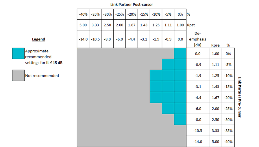
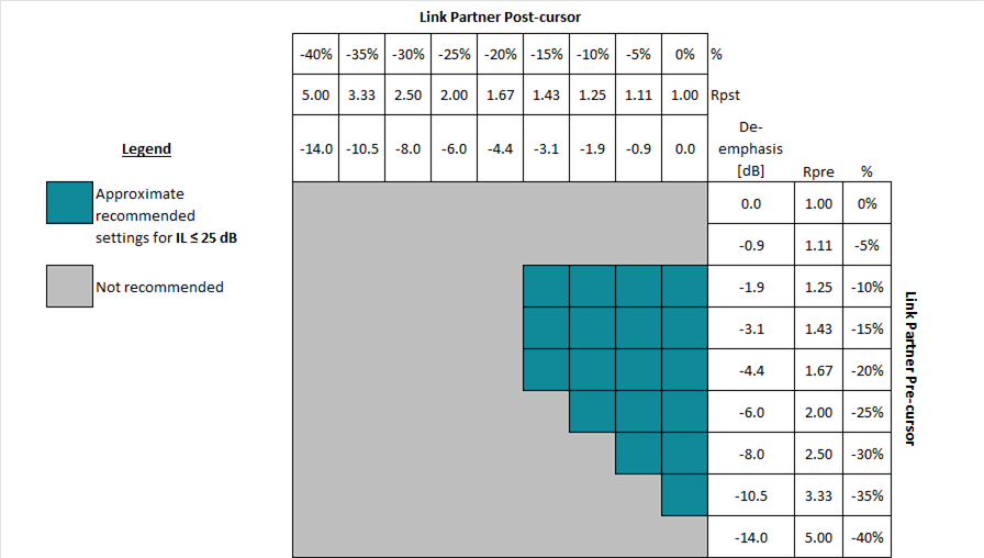
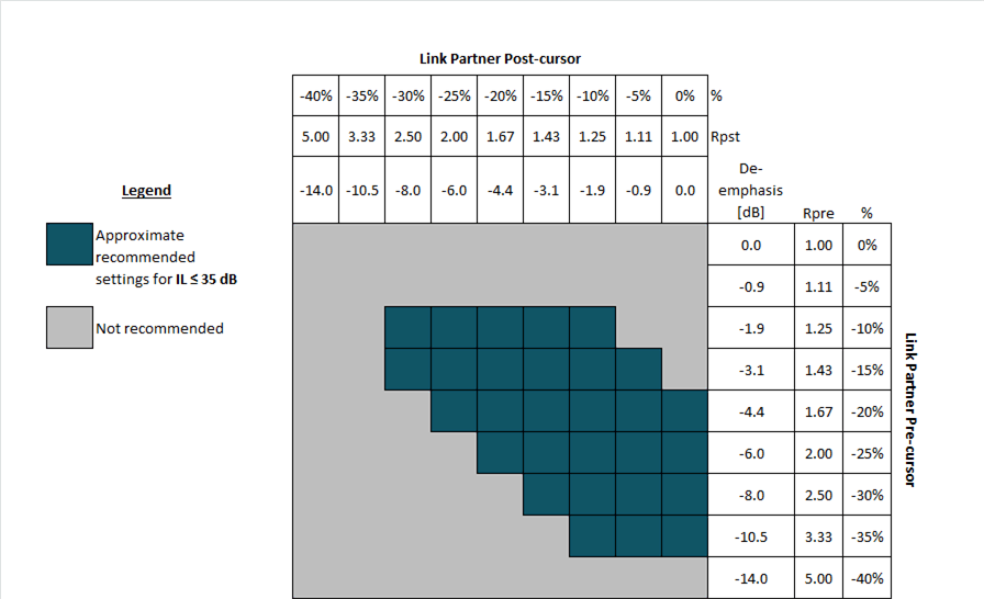
The recommended pre-cursor and post-cursor settings for a given channel will depend on the channel characteristics (mainly insertion loss) as well as the equalization capabilities of the downstream receiver. The DS250DF810 receiver, with its highly-capable CTLE and DFE, does not require a significant amount of pre- or post-cursor. The figures below give general recommendations for pre- and post-cursor for different channel loss conditions. The insertion loss (IL) in these plots refers to the total loss between the link partner transmitter and the DS250DF810 receiver.
 Figure 11. Guideline for link partner FIR settings when IL ≤ 15dB
  Figure 12. Guideline for link partner FIR settings when IL ≤ 25dB
  Figure 13. Guideline for link partner FIR settings when IL ≤ 35dB