SNLS401C February 2012 – September 2018 DS90C187
PRODUCTION DATA.
- 1 Features
- 2 Applications
- 3 Description
- 4 Revision History
- 5 Description (continued)
- 6 Pin Configuration and Functions
- 7 Specifications
-
8 Detailed Description
- 8.1 Overview
- 8.2 Functional Block Diagrams
- 8.3
Device Functional Modes
- 8.3.1 Device Configuration
- 8.3.2 Single Pixel Input / Single Pixel Output
- 8.3.3 Single Pixel Input / Dual Pixel Output
- 8.3.4 Dual Pixel Input / Dual Pixel Output
- 8.3.5 Pixel Clock Edge Select (RFB)
- 8.3.6 Power Management
- 8.3.7 Sleep Mode (PDB)
- 8.3.8 LVDS Outputs
- 8.3.9 18 bit / 24 bit Color Mode (18B)
- 8.3.10 LVCMOS Inputs
- 8.4 Programming
- 9 Application and Implementation
- 10Power Supply Recommendations
- 11Layout
- 12Device and Documentation Support
- 13Mechanical, Packaging, and Orderable Information
Package Options
Mechanical Data (Package|Pins)
- NLA|92
Thermal pad, mechanical data (Package|Pins)
Orderable Information
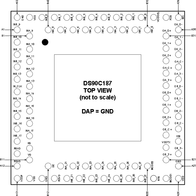
6 Pin Configuration and Functions
NLA Package
92-Pin VQFN-MR
Top View

DS90C187 Pin Descriptions — Serializer
| NAME | PIN NO. | I/O | DESCRIPTION |
|---|---|---|---|
| 1.8-V LVCMOS VIDEO INPUTS | |||
| INA_[27:21]
INA_[17:9] NA_[8:0] |
B19-B13,
B9-B1, B40-B32 |
I | Channel A Data Inputs
Typically consists of 8 Red, 8 Green, 8 Blue and a general purpose or L/R control bit. Includes pull down. |
| INB_[27:21]
INB_[17:14], INB_[13:9] INB_[8:0 |
A23-A17,
A10-A7, A5-A1, A50-A42 |
I | Channel B Data Inputs
Typically consists of 8 Red, 8 Green, 8 Blue and a general purpose or L/R control bit. Includes pull down. |
| HS (INA_18),
VS (INA_19), DE (INA_20) |
B10,
B11 B12 |
I | Video Control Signal Inputs -
HS = Horizontal Sync, VS = Vertical SYNC, and DE = Data Enable |
| IN_CLK | A6 | I | Pixel Input Clock
Includes pull down. |
| 1.8-V LVCMOS CONTROL INPUTS | |||
| MODE0,
MODE1 |
B20,
A25 |
I | Mode Control Input (MODE0)
00 = Single In / Single Out 01 = Single In / Dual Out 10 = Dual In / Dual Out 11 = Reserved Includes pull down. |
| RFB | A24 | I | Rising / Falling Clock Edge Select Input -
0 = Falling Edge, 1 = Rising Edge Includes pull down. |
| PDB | A40 | I | Power Down (Sleep) Control Input -
0 = Sleep (Power Down mode), 1 = device active (enabled) Includes pull down. |
| 18B | A29 | I | 18 bit / 24 bit Control Input -
0 = 24 bit mode, 1 = 18 bit mode Includes pull down. |
| VODSEL | A41 | I | VOD Level Select Input -
0 = Low swing, 1 = Normal swing Includes pull down. |
| N/C | A39 | I | no connect pin — leave open |
| RSVD | A11, A12, A16 | I | Reserved - Tie to Ground. |
| LVDS OUTPUTS | |||
| OA_C+
OA_C- |
B28,
A35 |
O | Channel A LVDS Output Clock —
Expects 100 Ω DC load. |
| OA_[3:0]+,
OA_[3:0]- |
B27, B29-B31
A34, A36-A38 |
O | Channel A LVDS Output Data —
Expects 100 Ω DC load. |
| OB_C+,
OB_C- |
B23,
A30 |
O | Channel B LVDS Output Clock —
Expects 100 Ω DC load. |
| OB_[3:0]+,
OB_[3:0]- |
B21, B24-B26
A28, A16-A33 |
O | Channel B LVDS Output Data —
Expects 100 Ω DC load. |
| POWER AND GROUND | |||
| VDDTX | B22 | P | Power supply for LVDS Drivers, 1.8V. |
| VDD | A14, A26, A51 | P | Power supply pin for core, 1.8V. |
| VDDP | A13 | P | Power supply pin for PLL, 1.8V. |
| GND | A15, A27, A52 | G | Ground pins. |
| DAP | DAP | G | Connect DAP to Ground plane. |