SNLS499D April 2016 – October 2019 DS90UB914A-Q1
PRODUCTION DATA.
- 1 Features
- 2 Applications
- 3 Description
- 4 Revision History
- 5 Device Comparison Table
- 6 Pin Configuration and Functions
-
7 Specifications
- 7.1 Absolute Maximum Ratings
- 7.2 ESD Ratings
- 7.3 Recommended Operating Conditions
- 7.4 Thermal Information
- 7.5 Electrical Characteristics
- 7.6 AC Timing Specifications (SCL, SDA) - I2C-Compatible
- 7.7 Bidirectional Control Bus DC Timing Specifications (SCL, SDA) - I2C-Compatible
- 7.8 Deserializer Switching Characteristics
- 7.9 Typical Characteristics
- 8 Parameter Measurement Information
-
9 Detailed Description
- 9.1 Overview
- 9.2 Functional Block Diagram
- 9.3
Feature Description
- 9.3.1 Serial Frame Format
- 9.3.2 Line Rate Calculations for the DS90UB913A/914A
- 9.3.3 Deserializer Multiplexer Input
- 9.3.4 Error Detection
- 9.3.5 Synchronizing Multiple Cameras
- 9.3.6 General-Purpose I/O (GPIO) Descriptions
- 9.3.7 LVCMOS VDDIO Option
- 9.3.8 EMI Reduction
- 9.3.9 Pixel Clock Edge Select (TRFB / RRFB)
- 9.3.10 Power Down
- 9.4
Device Functional Modes
- 9.4.1 DS90UB913A/914A Operation With External Oscillator as Reference Clock
- 9.4.2 DS90UB913A/914A Operation With Pixel Clock From Imager as Reference Clock
- 9.4.3 MODE Pin on Deserializer
- 9.4.4 Clock-Data Recovery Status Flag (LOCK), Output Enable (OEN) and Output State Select (OSS_SEL)
- 9.4.5 Built-In Self Test
- 9.4.6 BIST Configuration and Status
- 9.4.7 Sample BIST Sequence
- 9.5 Programming
- 9.6 Register Maps
- 10Application and Implementation
- 11Power Supply Recommendations
- 12Layout
- 13Device and Documentation Support
- 14Mechanical, Packaging, and Orderable Information
Package Options
Mechanical Data (Package|Pins)
- RHS|48
Thermal pad, mechanical data (Package|Pins)
- RHS|48
Orderable Information
9.3.5 Synchronizing Multiple Cameras
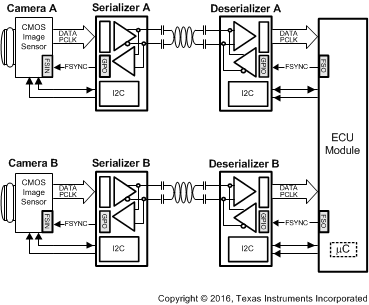
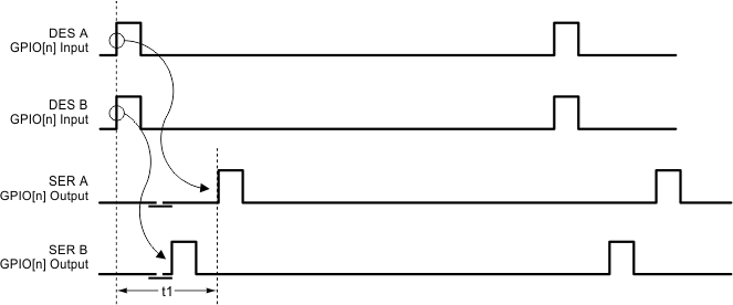
For applications requiring multiple cameras for frame-synchronization, it is recommended to utilize the General Purpose Input/Output (GPIO) pins to transmit control signals to synchronize multiple cameras together. To synchronize the cameras properly, the system controller needs to provide a field sync output (such as a vertical or frame sync signal) and the cameras must be set to accept an auxiliary sync input. The vertical synchronize signal corresponds to the start and end of a frame and the start and end of a field. Note this form of synchronization timing relationship has a non-deterministic latency. After the control data is reconstructed from the bidirectional control channel, there will be a time variation of the GPIO signals arriving at the different target devices (between the parallel links). The maximum latency delta (t1) of the GPIO data transmitted across multiple links is 25 µs.
NOTE
The user must verify that the timing variations between the different links are within their system and timing specifications.
See Figure 13 for an example of this function.
The maximum time (t1) between the rising edge of GPIO (that is, sync signal) to the time the signal arrives at Camera A and Camera B is 25 µs.
 Figure 13. Synchronizing Multiple Cameras
  Figure 14. GPIO Delta Latency