SNLS336J October 2010 – November 2014 DS90UH925Q-Q1
PRODUCTION DATA.
- 1 Features
- 2 Applications
- 3 Description
- 4 Revision History
- 5 Pin Configuration and Functions
-
6 Specifications
- 6.1 Absolute Maximum Ratings
- 6.2 Handling Ratings
- 6.3 Recommended Operating Conditions
- 6.4 Thermal Information
- 6.5 DC Electrical Characteristics
- 6.6 AC Electrical Characteristics
- 6.7 DC and AC Serial Control Bus Characteristics
- 6.8 Recommended Timing for Serial Control Bus
- 6.9 Switching Characteristics
- 6.10 Typical Charateristics
-
7 Detailed Description
- 7.1 Overview
- 7.2 Functional Block Diagram
- 7.3
Feature Description
- 7.3.1 High Speed Forward Channel Data Transfer
- 7.3.2 Low Speed Back Channel Data Transfer
- 7.3.3 Backward Compatible Mode
- 7.3.4 Common Mode Filter Pin (CMF)
- 7.3.5 Video Control Signal Filter
- 7.3.6 Power Down (PDB)
- 7.3.7 Remote Auto Power Down Mode
- 7.3.8 LVCMOS VDDIO Option
- 7.3.9 Input PCLK Loss Detect
- 7.3.10 Serial Link Fault Detect
- 7.3.11 Pixel Clock Edge Select (RFB)
- 7.3.12 Low Frequency Optimization (LFMODE)
- 7.3.13 Interrupt Pin — Functional Description and Usage (INTB)
- 7.3.14 EMI Reduction Features
- 7.4 Device Functional Modes
- 7.5 Programming
- 7.6 Register Maps
- 8 Applications and Implementation
- 9 Power Supply Recommendations
- 10Layout
- 11Device and Documentation Support
- 12Mechanical, Packaging, and Orderable Information
Package Options
Mechanical Data (Package|Pins)
- RHS|48
Thermal pad, mechanical data (Package|Pins)
- RHS|48
Orderable Information
7 Detailed Description
7.1 Overview
The DS90UH925Q-Q1 serializer transmits a 35-bit symbol over a single serial FPD-Link III pair operating up to 2.975 Gbps line rate. The serial stream contains an embedded clock, video control signals and DC-balanced video data and audio data which enhance signal quality to support AC coupling. The DS90UH925Q-Q1 serializes video and audio data then applies encryption through a High-Bandwidth Digital Content Protection (HDCP) Cipher and transmits out through the FPD-Link III interface. Audio encryption is supported. The serializer also includes the HDCP cipher. On board non-volatile memory stores the HDCP keys. All key exchange is conducted over the FPD-Link III bidirectional control interface. The serializer is intended for use with the DS90UH926Q-Q1 deserializer, but is also backward compatible with DS90UR906Q or DS90UR908Q FPD-Link II deserializer.
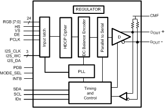
7.2 Functional Block Diagram
7.3 Feature Description
7.3.1 High Speed Forward Channel Data Transfer
The High Speed Forward Channel (HS_FC) is composed of 35 bits of data containing RGB data, sync signals, HDCP, I2C, and I2S audio transmitted from Serializer to Deserializer. Figure 11 illustrates the serial stream per PCLK cycle. This data payload is optimized for signal transmission over an AC coupled link. Data is randomized, balanced and scrambled.
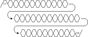 Figure 11. FPD-Link III Serial Stream
The device supports clocks in the range of 5 MHz to 85 MHz. The application payload rate is 2.975 Gbps maximum (175 Mbps minimum) with the actual line rate of 2.975 Gbps maximum and 525 Mbps Minimum.
7.3.2 Low Speed Back Channel Data Transfer
The Low-Speed Backward Channel (LS_BC) of the DS90UH925Q-Q1 provides bidirectional communication between the display and host processor. The information is carried back from the Deserializer to the Serializer per serial symbol. The back channel control data is transferred over the single serial link along with the high-speed forward data, DC balance coding and embedded clock information. This architecture provides a backward path across the serial link together with a high speed forward channel. The back channel contains the I2C, HDCP, CRC and 4 bits of standard GPIO information with 10 Mbps line rate.
7.3.3 Backward Compatible Mode
The DS90UH925Q-Q1 is also backward compatible to DS90UR906Q and DS90UR908Q FPD Link II deserializers at 5-65 MHz of PCLK. It transmits 28-bits of data over a single serial FPD-Link II pair operating at the line rate of 140 Mbps to 1.82 Gbps. The backward configuration mode can be set via MODE_SEL pin (Table 4) or the configuration register (Table 6). Note: frequency range = 15 - 65MHz when LFMODE = 0 and frequency range = 5 - <15MHz when LFMODE = 1.
7.3.4 Common Mode Filter Pin (CMF)
The serializer provides access to the center tap of the internal termination. A capacitor must be placed on this pin for additional common-mode filtering of the differential pair. This can be useful in high noise environments for additional noise rejection capability. A 0.1 μF capacitor must be connected to this pin to Ground.
7.3.5 Video Control Signal Filter
When operating the devices in Normal Mode, the Video Control Signals (DE, HS, VS) have the following restrictions:
- Normal Mode with Control Signal Filter Enabled: DE and HS — Only 2 transitions per 130 clock cycles are transmitted, the transition pulse must be 3 PCLK or longer.
- Normal Mode with Control Signal Filter Disabled: DE and HS — Only 2 transitions per 130 clock cycles are transmitted, no restriction on minimum transition pulse.
- VS — Only 1 transition per 130 clock cycles are transmitted, minimum pulse width is 130 clock cycles.
Video Control Signals are defined as low frequency signals with limited transitions. Glitches of a control signal can cause a visual display error. This feature allows for the chipset to validate and filter out any high frequency noise on the control signals. See Figure 12.
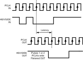 Figure 12. Video Control Signal Filter Waveform
7.3.6 Power Down (PDB)
The Serializer has a PDB input pin to ENABLE or POWER DOWN the device. This pin can be controlled by the host or through the VDDIO, where VDDIO = 3.0V to 3.6V or VDD33. To save power disable the link when the display is not needed (PDB = LOW). When the pin is driven by the host, make sure to release it after VDD33 and VDDIO have reached final levels; no external components are required. In the case of driven by the VDDIO = 3.0V to 3.6V or VDD33 directly, a 10 kohm resistor to the VDDIO = 3.0V to 3.6V or VDD33 , and a >10uF capacitor to the ground are required see Figure 23.
7.3.7 Remote Auto Power Down Mode
The Serializer features a remote auto power down mode. During the power down mode of the pairing deserializer, the Serializer enters the remote auto power down mode. In this mode, the power dissipation of the Serializer is reduced significantly. When the Deserializer is powered up, the Serializer enters the normal power on mode automatically. This feature is enabled through the register bit 0x01[7] Table 6.
7.3.8 LVCMOS VDDIO Option
1.8V or 3.3V Inputs and Outputs are powered from a separate VDDIO supply to offer compatibility with external system interface signals. Note: When configuring theVDDIO power supplies, all the single-ended data and control input pins for device need to scale together with the same operating VDDIO levels.
7.3.9 Input PCLK Loss Detect
The serializer can be programmed to enter a low power SLEEP state when the input clock (PCLK) is lost. A clock loss condition is detected when PCLK drops below approximately 1MHz. When a PCLK is detected again, the serializer will then lock to the incoming PCLK. Note – when PCLK is lost, the Serial Control Bus Registers values are still RETAINED.
7.3.10 Serial Link Fault Detect
The serial link fault detection is able to detect any of following seven (7) conditions
- cable open
- “+” to “-“ short
- “+” short to GND
- “-“ short to GND
- “+” short to battery
- “-“ short to battery
- Cable is linked correctly
If any one of the fault conditions occurs, The Link Detect Status is 0 (cable is not detected) on bit 0 of address 0x0C Table 6.
7.3.11 Pixel Clock Edge Select (RFB)
The RFB control register bit selects which edge of the Pixel Clock is used. For the serializer, this pin determines the edge that the data is latched on. If RFB is HIGH (‘1’), data is latched on the Rising edge of the PCLK. If RFB is LOW (‘0’), data is latched on the Falling edge of the PCLK.
7.3.12 Low Frequency Optimization (LFMODE)
The LFMODE is set via register (0x04[1:0]) or MODE_SEL Pin 24 (Table 4). It controls the operating frequency of the serializer. If LFMODE is Low (default), the PCLK frequency is between 15 MHz and 85 MHz. If LFMODE is High, the PCLK frequency is between 5 MHz and <15 MHz. Please note when the device LFMODE is changed, a PDB reset is required.
7.3.13 Interrupt Pin — Functional Description and Usage (INTB)
- On DS90UH925Q-Q1, set register 0xC6[5] = 1 and 0xC6[0] = 1
- DS90UH926Q-Q1 deserializer INTB_IN (pin 16) is set LOW by some downstream device.
- DS90UH925Q-Q1 serializer pulls INTB (pin 31) LOW. The signal is active low, so a LOW indicates an interrupt condition.
- External controller detects INTB = LOW; to determine interrupt source, read HDCP_ISR register .
- A read to HDCP_ISR will clear the interrupt at the DS90UH925Q-Q1, releasing INTB.
- The external controller typically must then access the remote device to determine downstream interrupt source and clear the interrupt driving INTB_IN. This would be when the downstream device releases the INTB_IN (pin 16) on the DS90UH926Q-Q1. The system is now ready to return to step (1) at next falling edge of INTB_IN.
7.3.14 EMI Reduction Features
7.3.14.1 Input SSC Tolerance (SSCT)
The DS90UH925Q-Q1 serializer is capable of tracking a triangular input spread spectrum clocking (SSC) profile up to +/-2.5% amplitude deviations (center spread), up to 35 kHz modulation at 5–85 MHz, from a host source.
7.3.14.2 GPIO[3:0] and GPO_REG[8:4]
In 18-bit RGB operation mode, the optional R[1:0] and G[1:0] of the DS90UH925Q-Q1 can be used as the general purpose IOs GPIO[3:0] in either forward channel (Inputs) or back channel (Outputs) application.
7.3.14.2.1 GPIO[3:0] Enable Sequence
See Table 1 for the GPIO enable sequencing.
Step 1: Enable the 18-bit mode either through the configuration register bit Table 6 on DS90UH925Q-Q1 only. DS90UH926Q-Q1 is automatically configured as in the 18-bit mode.
Step 2: To enable GPIO3 forward channel, write 0x03 to address 0x0F on DS90UH925Q-Q1, then write 0x05 to address 0x1F on DS90UH926Q-Q1.
Table 1. GPIO Enable Sequencing Table
| # | DESCRIPTION | DEVICE | FORWARD CHANNEL |
BACK CHANNEL |
|---|---|---|---|---|
| 1 | Enable 18-bit mode | DS90UH925Q-Q1 | 0x12 = 0x04 | 0x12 = 0x04 |
| DS90UH926Q-Q1 | Auto Load from DS90UH925Q-Q1 | Auto Load from DS90UH925Q-Q1 | ||
| 2 | GPIO3 | DS90UH925Q-Q1 | 0x0F = 0x03 | 0x0F = 0x05 |
| DS90UH926Q-Q1 | 0x1F = 0x05 | 0x1F = 0x03 | ||
| 3 | GPIO2 | DS90UH925Q-Q1 | 0x0E = 0x30 | 0x0E = 0x50 |
| DS90UH926Q-Q1 | 0x1E = 0x50 | 0x1E = 0x30 | ||
| 4 | GPIO1 | DS90UH925Q-Q1 | 0x0E = 0x03 | 0x0E = 0x05 |
| DS90UH926Q-Q1 | 0x1E = 0x05 | 0x1E = 0x03 | ||
| 5 | GPIO0 | DS90UH925Q-Q1 | 0x0D = 0x93 | 0x0D = 0x95 |
| DS90UH926Q-Q1 | 0x1D = 0x95 | 0x1D = 0x93 |
7.3.14.2.2 GPO_REG[8:4] Enable Sequence
GPO_REG[8:4] are the outputs only pins. They must be programmed through the local register bits. See Table 2 for the GPO_REG enable sequencing.
Step 1: Enable the 18-bit mode either through the configuration register bit Table 6 on DS90UH925Q-Q1 only. DS90UH926Q-Q1 is automatically configured as in the 18-bit mode.
Step 2: To enable GPO_REG8 outputs an “1”, write 0x90 to address 0x11 on DS90UH925Q-Q1.
Table 2. GPO_REG Enable Sequencing Table
| # | DESCRIPTION | DEVICE | LOCAL ACCESS |
LOCAL OUTPUT |
|---|---|---|---|---|
| 1 | Enable 18-bit mode | DS90UH925Q-Q1 | 0x12 = 0x04 | |
| 2 | GPO_REG8 | DS90UH925Q-Q1 | 0x11 = 0x90 | “1” |
| 0x11 = 0x10 | “0” | |||
| 3 | GPO_REG7 | DS90UH925Q-Q1 | 0x11 = 0x09 | “1” |
| 0x11 = 0x01 | “0” | |||
| 4 | GPO_REG6 | DS90UH925Q-Q1 | 0x10 = 0x90 | “1” |
| 0x10 = 0x10 | “0” | |||
| 5 | GPO_REG5 | DS90UH925Q-Q1 | 0x10 = 0x09 | “1” |
| 0x10 = 0x01 | “0” | |||
| 6 | GPO_REG4 | DS90UH925Q-Q1 | 0x0F = 0x90 | “1” |
| 0x0F = 0x10 | “0” |
7.3.14.3 I2S Transmitting
In normal 24-bit RGB operation mode, the DS90UH925Q-Q1 supports 3 bits of I2S. They are I2S_CLK, I2S_WC and I2S_DA. The optionally encrypted and packetized audio information can be transmitted during the video blanking (data island transport) or during active video (forward channel frame transport). Note: The bit rates of any I2S bits must maintain one fourth of the PCLK rate. The audio encryption capability is supported per HDCP v1.3.
7.3.14.3.1 Secondary I2S Channel
In I2S Channel B operation mode, the secondary I2S data (I2S_DB) can be used as the additional I2S audio in addition to the 3–bit of I2S. The I2S_DB input must be synchronized to I2S_CLK and aligned with I2S_DA and I2S_WC at the input to the serializer. This operation mode is enabled through either the MODE_SEL pin (Table 4) or through the register bit 0x12[0] (Table 6). Table 3 below covers the range of I2S sample rates.
Table 3. Audio Interface Frequencies
| SAMPLE RATE (kHz) | I2S DATA WORD SIZE (bits) | I2S CLK (MHz) |
|---|---|---|
| 32 | 16 | 1.024 |
| 44.1 | 16 | 1.411 |
| 48 | 16 | 1.536 |
| 96 | 16 | 3.072 |
| 192 | 16 | 6.144 |
| 32 | 24 | 1.536 |
| 44.1 | 24 | 2.117 |
| 48 | 24 | 2.304 |
| 96 | 24 | 4.608 |
| 192 | 24 | 9.216 |
| 32 | 32 | 2.048 |
| 44.1 | 32 | 2.822 |
| 48 | 32 | 3.072 |
| 96 | 32 | 6.144 |
| 192 | 32 | 12.288 |
7.3.14.4 HDCP
The Cipher function is implemented in the serializer per HDCP v1.3 specification. The DS90UH925Q-Q1 provides HDCP encryption of audiovisual content when connected to an HDCP capable FPD-Link III deserializer such as the DS90UH926Q-Q1. HDCP authentication and shared key generation is performed using the HDCP Control Channel which is embedded in the forward and backward channels of the serial link. An on-chip Non-Volatile Memory (NVM) is used to store the HDCP keys. The confidential HDCP keys are loaded by TI during the manufacturing process and are not accessible external to the device.
The DS90UH925Q-Q1 uses the Cipher engine to encrypt the data as per HDCP v1.3. The encrypted data is transmitted through the FPD-Link III interface.
7.3.14.5 Built In Self Test (BIST)
An optional At-Speed Built In Self Test (BIST) feature supports the testing of the high speed serial link and the low- speed back channel. This is useful in the prototype stage, equipment production, in-system test and also for system diagnostics. Note: BIST not available in backwards compatible mode.
7.3.14.5.1 BIST Configuration and Status
The BIST mode is enabled at the deseralizer by the Pin select (Pin 44 BISTEN and Pin 16 BISTC) or configuration register (Table 6) through the deserializer. When LFMODE = 0, the pin based configuration defaults to external PCLK or 33 MHz internal Oscillator clock (OSC) frequency. In the absence of PCLK, the user can select the desired OSC frequency (default 33 MHz or 25MHz) through the register bit. When LFMODE = 1, the pin based configuration defaults to external PCLK or 12.5MHz MHz internal Oscillator clock (OSC) frequency.
When BISTEN of the deserializer is high, the BIST mode enable information is sent to the serializer through the Back Channel. The serializer outputs a test pattern and drives the link at speed. The deserializer detects the test pattern and monitors it for errors. The PASS output pin toggles to flag any payloads that are received with 1 to 35 bit errors.
The BIST status is monitored real time on PASS pin. The result of the test is held on the PASS output until reset (new BIST test or Power Down). A high on PASS indicates NO ERRORS were detected. A Low on PASS indicates one or more errors were detected. The duration of the test is controlled by the pulse width applied to the deserializer BISTEN pin. This BIST feature also contains a Link Error Count and a Lock Status. If the connection of the serial link is broken, then the link error count is shown in the register. When the PLL of the deserializer is locked or unlocked, the lock status can be read in the register. See Table 6.
7.3.14.5.1.1 Sample BIST Sequence
See Figure 13 for the BIST mode flow diagram.
Step 1: For the DS90UH925Q-Q1 and DS90UH926Q-Q1 FPD-Link III chipset, BIST Mode is enabled via the BISTEN pin of DS90UH926Q-Q1 FPD-Link III deserializer. The desired clock source is selected through BISTC pin.
Step 2: The DS90UH925Q-Q1 serializer is woken up through the back channel if it is not already on. The all zero pattern on the data pins is sent through the FPD-Link III to the deserializer. Once the serializer and the deserializer are in BIST mode and the deserializer acquires Lock, the PASS pin of the deserializer goes high and BIST starts checking the data stream. If an error in the payload (1 to 35) is detected, the PASS pin will switch low for one half of the clock period. During the BIST test, the PASS output can be monitored and counted to determine the payload error rate.
Step 3: To Stop the BIST mode, the deserializer BISTEN pin is set Low. The deserializer stops checking the data. The final test result is held on the PASS pin. If the test ran error free, the PASS output will be High. If there was one or more errors detected, the PASS output will be Low. The PASS output state is held until a new BIST is run, the device is RESET, or Powered Down. The BIST duration is user controlled by the duration of the BISTEN signal.
Step 4: The Link returns to normal operation after the deserializer BISTEN pin is low. Figure 14 shows the waveform diagram of a typical BIST test for two cases. Case 1 is error free, and Case 2 shows one with multiple errors. In most cases it is difficult to generate errors due to the robustness of the link (differential data transmission etc.), thus they may be introduced by greatly extending the cable length, faulting the interconnect, reducing signal condition enhancements (Rx Equalization).
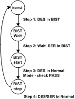 Figure 13. BIST Mode Flow Diagram
7.3.14.5.2 Forward Channel and Back Channel Error Checking
While in BIST mode, the serializer stops sampling RGB input pins and switches over to an internal all-zero pattern. The internal all-zeroes pattern goes through scrambler, dc-balancing etc. and goes over the serial link to the deserializer. The deserializer on locking to the serial stream compares the recovered serial stream with all-zeroes and records any errors in status registers and dynamically indicates the status on PASS pin. The deserializer then outputs a SSO pattern on the RGB output pins.
The back-channel data is checked for CRC errors once the serializer locks onto back-channel serial stream as indicated by link detect status (register bit 0x0C[0]). The CRC errors are recorded in an 8-bit register. The register is cleared when the serializer enters the BIST mode. As soon as the serializer exits BIST mode, the functional mode CRC register starts recording the CRC errors. The BIST mode CRC error register is active in BIST mode only and keeps the record of last BIST run until cleared or enters BIST mode again.
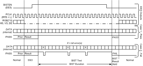 Figure 14. BIST Waveforms
7.3.14.6 Internal Pattern Generation
The DS90UH925Q-Q1 serializer supports the internal pattern generation feature. It allows basic testing and debugging of an integrated panel through the FPD-Link III output stream. The test patterns are simple and repetitive and allow for a quick visual verification of panel operation. As long as the device is not in power down mode, the test pattern will be displayed even if no parallel input is applied. If no PCLK is received, the test pattern can be configured to use a programmed oscillator frequency. For detailed information, refer to SNLA132.
7.4 Device Functional Modes
7.4.1 Configuration Select (MODE_SEL)
Configuration of the device may be done via the MODE_SEL input pin, or via the configuration register bit. A pull-up resistor and a pull-down resistor of suggested values may be used to set the voltage ratio of the MODE_SEL input (VR4) and VDD33 to select one of the other 10 possible selected modes. See Figure 15 and Table 4.
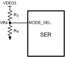 Figure 15. MODE_SEL Connection Diagram
Table 4. Configuration Select (MODE_SEL)
| # | IDEAL RATIO VR4/VDD33 |
IDEAL VR4
(V) |
SUGGESTED RESISTOR R3 kΩ (1% tol) |
SUGGESTED RESISTOR R4 kΩ (1% tol) |
LFMODE | REPEATER | BACKWARD COMPA- TIBLE |
I2S CHANNEL B (18–bit MODE) |
|---|---|---|---|---|---|---|---|---|
| 1 | 0 | 0 | Open | 40.2 or Any | L | L | L | L |
| 2 | 0.164 | 0.541 | 255 | 49.9 | L | H | L | L |
| 3 | 0.221 | 0.729 | 243 | 69.8 | L | H | L | H |
| 4 | 0.285 | 0.941 | 237 | 95.3 | H | L | L | L |
| 5 | 0.359 | 1.185 | 196 | 110 | H | L | L | H |
| 6 | 0.453 | 1.495 | 169 | 140 | H | H | L | L |
| 7 | 0.539 | 1.779 | 137 | 158 | H | H | L | H |
| 8 | 0.728 | 2.402 | 90.9 | 243 | H | L | H* | L |
| LFMODE: L = frequency range is 15 – 85 MHz (Default) H = frequency range is 5 – <15 MHz Repeater: L = Repeater OFF (Default) H = Repeater ON Backward Compatible: L = Backward Compatible is OFF (Default) H = Backward Compatible is ON; DES = DS90UR906Q or DS90UR916Q or DS90UR908Q – frequency range = 15 - 65 MHz when LFMODE = 0 – frequency range = 5 - <15 MHz when LFMODE = 1 I2S Channel B: L = I2S Channel B is OFF, Normal 24-bit RGB Mode (Default) H = I2S Channel B is ON, 18-bit RGB Mode with I2S_DB Enabled. Note: use of GPIO(s) on unused inputs must be enabled by register. |
||||||||
7.4.2 HDCP Repeater
When DS90UH925Q-Q1 and DS90UH926Q-Q1 are configured as the HDCP Repeater application, it provides a mechanism to extend HDCP transmission over multiple links to multiple display devices. This repeater application provides a mechanism to authenticate all HDCP Receivers in the system and distribute protected content to the HDCP Receivers using the encryption mechanisms provided in the HDCP specification.
7.4.3 Repeater Configuration
In HDCP repeater application, In this document, the DS90UH925Q-Q1 is referred to as the HDCP Transmitter or transmit port (TX), and the DS90UH926Q-Q1 is referred to as the HDCP Receiver (RX). Figure 16 shows the maximum configuration supported for HDCP Repeater implementations using the DS90UH925Q-Q1 (TX) and DS90UH926Q-Q1 (RX). Two levels of HDCP Repeaters are supported with a maximum of three HDCP Transmitters per HDCP Receiver.
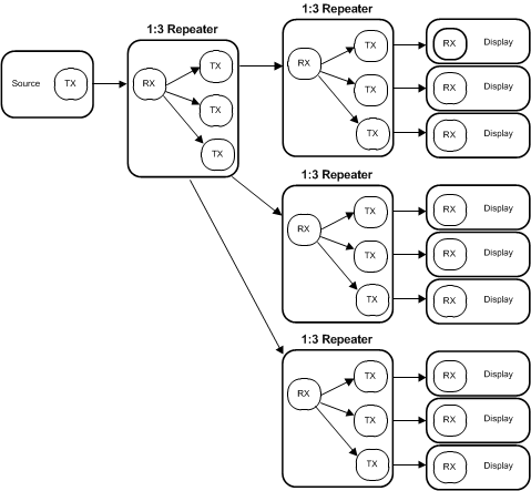 Figure 16. HDCP Maximum Repeater Application
To support HDCP Repeater operation, the DS90UH926Q-Q1 Deserializer includes the ability to control the downstream authentication process, assemble the KSV list for downstream HDCP Receivers, and pass the KSV list to the upstream HDCP Transmitter. An I2C master within the DS90UH926Q-Q1 communicates with the I2C slave within the DS90UH925Q-Q1 Serializer. The DS90UH925Q-Q1 Serializer handles authenticating with a downstream HDCP Receiver and makes status available through the I2C interface. The DS90UH926Q-Q1 monitors the transmit port status for each DS90UH925Q-Q1 and reads downstream KSV and KSV list values from the DS90UH925Q-Q1.
In addition to the I2C interface used to control the authentication process, the HDCP Repeater implementation includes two other interfaces. A parallel LVCMOS interface provides the unencrypted video data in 24-bit RGB format and includes the DE/VS/HS control signals. In addition to providing the RGB video data, the parallel LVCMOS interface communicates control information and packetized audio data during video blanking intervals. A separate I2S audio interface may optionally be used to send I2S audio data between the HDCP Receiver and HDCP Transmitter in place of using the packetized audio over the parallel LVCMOS interface. All audio and video data is decrypted at the output of the HDCP Receiver and is re-encrypted by the HDCP Transmitter.
Figure 17 provides more detailed block diagram of a 1:2 HDCP repeater configuration.
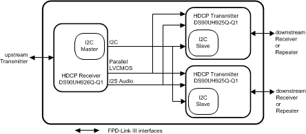 Figure 17. HDCP 1:2 Repeater Configuration
7.4.4 Repeater Connections
The HDCP Repeater requires the following connections between the HDCP Receiver and each HDCP Transmitter Figure 18.
- Video Data – Connect PCLK, RGB and control signals (DE, VS, HS).
- I2C – Connect SCL and SDA signals. Both signals should be pulled up to VDD33 with 4.7 kΩ resistors.
- Audio – Connect I2S_CLK, I2S_WC, and I2S_DA signals.
- IDx pin – Each HDCP Transmitter and Receiver must have an unique I2C address.
- MODE_SEL pin – All HDCP Transmitter and Receiver must be set into the Repeater Mode.
- Interrupt pin – Connect DS90UH926Q-Q1 INTB_IN pin to DS90UH925Q-Q1 INTB pin. The signal must be pulled up to VDDIO.
 Figure 18. HDCP Repeater Connection Diagram
7.5 Programming
7.5.1 Serial Control Bus
The DS90UH925Q-Q1 is configured by the use of a serial control bus that is I2C protocol compatible. This bus is also used by the Host source to control and monitor status of the HDCP function. Multiple serializer devices may share the serial control bus since 16 device addresses are supported. Device address is set via R1 and R2 values on IDx pin. See Figure 19 below.
The serial control bus consists of two signals and a configuration pin. The SCL is a Serial Bus Clock Input / Output. The SDA is the Serial Bus Data Input / Output signal. Both SCL and SDA signals require an external pull-up resistor to VDD33. For most applications a 4.7 k pull-up resistor to VDD33 may be used. The resistor value may be adjusted for capacitive loading and data rate requirements. The signals are either pulled High, or driven Low.
 Figure 19. Serial Control Bus Connection
The configuration pin is the IDx pin. This pin sets one of 9 possible device addresses. A pull-up resistor and a pull-down resistor of suggested values may be used to set the voltage ratio of the IDx input (VR2) and VDD33 to select one of the other 9 possible addresses. Table 5 defines the required VR2 and VR2/VDD33 ratios, and suggests standard resistor values to achieve these ratios. In systems where excessive noise may be present, we recommend reducing the resistor values (by a factor of 10x or 100x) while maintaining the required ratio. This provides tighter coupling to supply rails, and more stability of VR2 in the presence of coupled noise. Note that reducing the resistor values will increase the current consumed by the resistor divider. See Table 5.
Table 5. Serial Control Bus Addresses for IDx
| # | IDEAL RATIO VR2 / VDD33 |
IDEAL VR2
(V) |
SUGGESTED RESISTOR R1 kΩ (1% tol) |
SUGGESTED RESISTOR R2 kΩ (1% tol) |
ADDRESS 7'b | ADDRESS 8'b APPENDED |
|---|---|---|---|---|---|---|
| 1 | 0 | 0 | Open | 40.2 or Any | 0x0C | 0x18 |
| 2 | 0.121 | 0.399 | 294 | 40.2 | 0x0D | 0x1A |
| 3 | 0.152 | 0.502 | 280 | 49.9 | 0x0E | 0x1C |
| 4 | 0.180 | 0.594 | 137 | 30.1 | 0x0F | 0x1E |
| 5 | 0.208 | 0.685 | 118 | 30.9 | 0x10 | 0x20 |
| 6 | 0.303 | 0.999 | 115 | 49.9 | 0x13 | 0x26 |
| 7 | 0.345 | 1.137 | 102 | 53.6 | 0x14 | 0x28 |
| 8 | 0.389 | 1.284 | 115 | 73.2 | 0x15 | 0x2A |
| 9 | 0.727 | 2.399 | 90.9 | 243 | 0x1B | 0x36 |
The Serial Bus protocol is controlled by START, START-Repeated, and STOP phases. A START occurs when SCL transitions Low while SDA is High. A STOP occurs when SDA transition High while SCL is also HIGH. See Figure 20.
 Figure 20. START and STOP Conditions
To communicate with a remote device, the host controller (master) sends the slave address and listens for a response from the slave. This response is referred to as an acknowledge bit (ACK). If a slave on the bus is addressed correctly, it Acknowledges (ACKs) the master by driving the SDA bus low. If the address doesn't match a device's slave address, it Not-acknowledges (NACKs) the master by letting SDA be pulled High. ACKs also occur on the bus when data is being transmitted. When the master is writing data, the slave ACKs after every data byte is successfully received. When the master is reading data, the master ACKs after every data byte is received to let the slave know it wants to receive another data byte. When the master wants to stop reading, it NACKs after the last data byte and creates a stop condition on the bus. All communication on the bus begins with either a Start condition or a Repeated Start condition. All communication on the bus ends with a Stop condition. A READ is shown in Figure 21 and a WRITE is shown in Figure 22.
If the Serial Bus is not required, the three pins may be left open (NC).
 Figure 21. Serial Control Bus — READ
 Figure 22. Serial Control Bus — WRITE
7.6 Register Maps
Table 6. Serial Control Bus Registers
| ADD (dec) |
ADD (hex) |
REGISTER NAME | Bit(s) | REG- ISTER TYPE |
DEFAULT (hex) |
FUNCTION | DESCRIPTION |
|---|---|---|---|---|---|---|---|
| 0 | 0x00 | I2C Device ID | 7:1 | RW | Device ID | 7–bit address of Serializer | |
| 0 | RW | ID Setting | I2C ID Setting 1: Register I2C Device ID (Overrides IDx pin) 0: Device ID is from IDx pin |
||||
| 1 | 0x01 | Reset | 7 | RW | 0x00 | Remote Auto Power Down | Remote Auto Power Down 1: Power down when no Bidirectional Control Channel link is detected 0: Do not power down when no Bidirectional Control Channel link is detected |
| 6:2 | Reserved. | ||||||
| 1 | RW | Digital RESET1 | Reset the entire digital block including registers This bit is self-clearing. 1: Reset 0: Normal operation |
||||
| 0 | RW | Digital RESET0 | Reset the entire digital block except registers This bit is self-clearing 1: Reset 0: Normal operation |
||||
| 3 | 0x03 | Configuration [0] | 7 | RW | 0xD2 | Back channel CRC Checker Enable | Back Channel Check Enable 1: Enable 0: Disable |
| 6 | Reserved. | ||||||
| 5 | RW | I2C Remote Write Auto Acknowledge | Automatically Acknowledge I2C Remote Write When enabled, I2C writes to the Deserializer (or any remote I2C Slave, if I2C PASS ALL is enabled) are immediately acknowledged without waiting for the Deserializer to acknowledge the write. This allows higher throughput on the I2C bus 1: Enable 0: Disable |
||||
| 4 | RW | Filter Enable | HS, VS, DE two clock filter When enabled, pulses less than two full PCLK cycles on the DE, HS, and VS inputs will be rejected 1: Filtering enable 0: Filtering disable |
||||
| 3 | RW | I2C Pass-through | I2C Pass-Through Mode 1: Pass-Through Enabled 0: Pass-Through Disabled |
||||
| 2 | Reserved | ||||||
| 1 | RW | PCLK Auto | Switch over to internal OSC in the absence of PCLK 1: Enable auto-switch 0: Disable auto-switch |
||||
| 0 | RW | TRFB | Pixel Clock Edge Select 1: Parallel Interface Data is strobed on the Rising Clock Edge. 0: Parallel Interface Data is strobed on the Falling Clock Edge. |
||||
| 4 | 0x04 | Configuration [1] | 7 | RW | 0x80 | Failsafe State | Input Failsafe State 1: Failsafe to Low 0: Failsafe to High |
| 6 | Reserved | ||||||
| 5 | RW | CRC Error Reset | Clear back channel CRC Error Counters This bit is NOT self-clearing 1: Clear Counters 0: Normal Operation |
||||
| 4 | Reserved | ||||||
| 3 | RW | Backward Compatible select by pin or register control | Backward Compatible (BC) mode set by MODE_SEL pin or register 1: BC is set by register bit. Use register bit reg_0x04[2] to set BC Mode 0: BC is set by MODE_SEL pin. |
||||
| 2 | RW | Backward Compatible Mode Select | Backward compatible (BC) mode to DS90UR906Q or DS90UR908Q, if reg_0x04[3] = 1 1: Backward compatible with DS90UR906Q or DS90UR908Q 0: Backward Compatible is OFF (default) |
||||
| 1 | RW | LFMODE select by pin or register control | Frequency range is set by MODE_SEL pin or register 1: Frequency range is set by register. Use register bit reg_0x04[0] to set LFMODE 0: Frequency range is set by MODE_SEL pin. |
||||
| 0 | RW | LFMODE | Frequency range select 1: PCLK range = 5MHz - <15 MHz), if reg_0x04[1] = 1 0: PCLK range = 15MHz - 85MHz (default) |
||||
| 5 | 0x05 | I2C Control | 7:5 | 0x00 | Reserved | ||
| 4:3 | RW | SDA Output Delay | SDA output delay Configures output delay on the SDA output. Setting this value will increase output delay in units of 40ns. Nominal output delay values for SCL to SDA are 00: 240ns 01: 280ns 10: 320ns 11: 360ns |
||||
| 2 | RW | Local Write Disable | Disable remote writes to local registers Setting the bit to a 1 prevents remote writes to local device registers from across the control channel. It prevents writes to the Serializer registers from an I2C master attached to the Deserializer. Setting this bit does not affect remote access to I2C slaves at the Serializer |
||||
| 1 | RW | I2C Bus Timer Speedup | Speed up I2C bus watchdog timer 1: Watchdog timer expires after ~50 ms. 0: Watchdog Timer expires after ~1 s |
||||
| 0 | RW | I2C Bus timer Disable | Disable I2C bus watchdog timer When the I2C watchdog timer may be used to detect when the I2C bus is free or hung up following an invalid termination of a transaction. If SDA is high and no signalling occurs for ~1 s, the I2C bus assumes to be free. If SDA is low and no signaling occurs, the device attempts to clear the bus by driving 9 clocks on SCL |
||||
| 6 | 0x06 | DES ID | 7:1 | RW | 0x00 | DES Device ID | 7-bit Deserializer Device ID Configures the I2C Slave ID of the remote Deserializer. A value of 0 in this field disables I2C access to the remote Deserializer. This field is automatically configured by the Bidirectional Control Channel once RX Lock has been detected. Software may overwrite this value, but should also assert the FREEZE DEVICE ID bit to prevent overwriting by the Bidirectional Control Channel. |
| 0 | RW | Device ID Frozen | Freeze Deserializer Device ID Prevents autoloading of the Deserializer Device ID by the Bidirectional Control Channel. The ID will be frozen at the value written. |
||||
| 7 | 0x07 | Slave ID | 7:1 | RW | 0X00 | Slave Device ID | 7-bit Remote Slave Device ID Configures the physical I2C address of the remote I2C Slave device attached to the remote Deserializer. If an I2C transaction is addressed to the Slave Device Alias ID, the transaction will be remapped to this address before passing the transaction across the Bidirectional Control Channel to the Deserializer |
| 0 | Reserved | ||||||
| 8 | 0x08 | Slave Alias | 7:1 | RW | 0x00 | Slave Device Alias ID | 7-bit Remote Slave Device Alias ID Assigns an Alias ID to an I2C Slave device attached to the remote Deserializer. The transaction will be remapped to the address specified in the Slave ID register. A value of 0 in this field disables access to the remote I2C Slave. |
| 0 | Reserved | ||||||
| 10 | 0x0A | CRC Errors | 7:0 | R | 0x00 | CRC Error LSB | Number of back channel CRC errors – 8 least significant bits |
| 11 | 0x0B | 7:0 | R | 0x00 | CRC Error MSB | Number of back channel CRC errors – 8 most significant bits | |
| 12 | 0x0C | General Status | 7:4 | 0x00 | Reserved | ||
| 3 | R | BIST CRC Error | Back channel CRC error during BIST communication with Deserializer. The bit is cleared upon loss of link, restart of BIST, or assertion of CRC ERROR RESET in register 0x04. |
||||
| 2 | R | PCLK Detect | PCLK Status 1: Valid PCLK detected 0: Valid PCLK not detected |
||||
| 1 | R | DES Error | Back channel CRC error during communication with Deserializer. The bit is cleared upon loss of link or assertion of CRC ERROR RESET in register 0x04. |
||||
| 0 | R | LINK Detect | LINK Status 1: Cable link detected 0: Cable link not detected (Fault Condition) |
||||
| 13 | 0x0D | Revision ID and GPIO0 Configuration | 7:4 | R | 0xA0 | Rev-ID | Revision ID: 1010 Production Device |
| 3 | RW | GPIO0 Output Value | Local GPIO output value This value is output on the GPIO pin when the GPIO function is enabled, the local GPIO direction is Output, and remote GPIO control is disabled. |
||||
| 2 | RW | GPIO0 Remote Enable | Remote GPIO control 1: Enable GPIO control from remote Deserializer. The GPIO pin will be an output, and the value is received from the remote Deserializer. 0: Disable GPIO control from remote Deserializer. |
||||
| 1 | RW | GPIO0 Direction | Local GPIO Direction 1: Input 0: Output |
||||
| 0 | RW | GPIO0 Enable | GPIO function enable 1: Enable GPIO operation 0: Enable normal operation |
||||
| 14 | 0x0E | GPIO2 and GPIO1 Configurations | 7 | RW | 0x0 | GPIO2 Output Value | Local GPIO output value This value is output on the GPIO pin when the GPIO function is enabled, the local GPIO direction is Output, and remote GPIO control is disabled. |
| 6 | RW | GPIO2 Remote Enable | Remote GPIO control 1: Enable GPIO control from remote Deserializer. The GPIO pin will be an output, and the value is received from the remote Deserializer. 0: Disable GPIO control from remote Deserializer. |
||||
| 5 | RW | GPIO2 Direction | Local GPIO Direction 1: Input 0: Output |
||||
| 4 | RW | GPIO2 Enable | GPIO function enable 1: Enable GPIO operation 0: Enable normal operation |
||||
| 3 | RW | GPIO1 Output Value | Local GPIO output value This value is output on the GPIO pin when the GPIO function is enabled, the local GPIO direction is Output, and remote GPIO control is disabled. |
||||
| 2 | RW | GPIO1 Remote Enable | Remote GPIO control 1: Enable GPIO control from remote Deserializer. The GPIO pin will be an output, and the value is received from the remote Deserializer. 0: Disable GPIO control from remote Deserializer. |
||||
| 1 | RW | GPIO1 Direction | Local GPIO Direction 1: Input 0: Output |
||||
| 0 | RW | GPIO1 Enable | GPIO function enable 1: Enable GPIO operation 0: Enable normal operation |
||||
| 15 | 0x0F | GPO_REG4 and GPIO3 Configurations | 7 | RW | 0x00 | GPO_REG4 Output Value | Local GPO_REG4 output value This value is output on the GPO pin when the GPO function is enabled. (The local GPO direction is Output, and remote GPO control is disabled) |
| 6:5 | Reserved | ||||||
| 4 | RW | GPO_REG4 Enable | GPO_REG4 function enable 1: Enable GPO operation 0: Enable normal operation |
||||
| 3 | RW | GPIO3 Output Value | Local GPIO output value This value is output on the GPIO pin when the GPIO function is enabled, the local GPIO direction is Output, and remote GPIO control is disabled. |
||||
| 2 | RW | GPIO3 Remote Enable | Remote GPIO control 1: Enable GPIO control from remote Deserializer. The GPIO pin will be an output, and the value is received from the remote Deserializer. 0: Disable GPIO control from remote Deserializer. |
||||
| 1 | RW | GPIO3 Direction | Local GPIO Direction 1: Input 0: Output |
||||
| 0 | RW | GPIO3 Enable | GPIO function enable 1: Enable GPIO operation 0: Enable normal operation |
||||
| 16 | 0x10 | GPO_REG6 and GPO_REG5 Configurations | 7 | RW | 0x00 | GPO_REG6 Output Value | Local GPO_REG6 output value This value is output on the GPO pin when the GPO function is enabled. (The local GPO direction is Output, and remote GPO control is disabled) |
| 6:5 | Reserved | ||||||
| 4 | RW | GPO_REG6 Enable | GPO_REG6 function enable 1: Enable GPO operation 0: Enable normal operation |
||||
| 3 | RW | GPO_REG5 Output Value | Local GPO_REG5 output value This value is output on the GPO pin when the GPO function is enabled, the local GPO direction is Output, and remote GPO control is disabled. |
||||
| 2:1 | Reserved | ||||||
| 0 | RW | GPO_REG5 Enable | GPO_REG5 function enable 1: Enable GPO operation 0: Enable normal operation |
||||
| 17 | 0x11 | GPO_REG8 and GPO_REG7 Configurations | 7 | RW | 0x00 | GPO_REG8 Output Value | Local GPO_REG8 output value This value is output on the GPO pin when the GPO function is enabled. (The local GPO direction is Output, and remote GPO control is disabled) |
| 6:5 | Reserved | ||||||
| 4 | RW | GPO_REG8 Enable | GPO_REG8 function enable 1: Enable GPO operation 0: Enable normal operation |
||||
| 3 | RW | GPO_REG7 Output Value | Local GPO_REG7 output value This value is output on the GPO pin when the GPO function is enabled, the local GPO direction is Output, and remote GPO control is disabled. |
||||
| 2:1 | Reserved | ||||||
| 0 | RW | GPO_REG7 Enable | GPO_REG7 function enable 1: Enable GPO operation 0: Enable normal operation |
||||
| 18 | 0x12 | Data Path Control | 7 | 0x00 | Reserved | ||
| 6 | RW | Pass RGB | Setting this bit causes RGB data to be sent independent of DE. It allows operation in systems which may not use DE to frame video data or send other data when DE is de-asserted. Note that setting this bit prevents HDCP operation and blocks packetized audio. This bit does not need to be set in Backwards Compatible mode 1: Pass RGB independent of DE 0: Normal operation (DE gates RGB data transmission - RGB data is transmitted only when DE is active) |
||||
| 5 | RW | DE Polarity | The bit indicates the polarity of the Data Enable (DE) signal. 1: DE is inverted (active low, idle high) 0: DE is positive (active high, idle low) |
||||
| 4 | RW | I2S Repeater Regeneration | I2S Repeater Regeneration 1: Repeater regenerate I2S from I2S pins 0: Repeater pass through I2S from video pins |
||||
| 3 | RW | I2S Channel B Enable Override | I2S Channel B Enable 1: Set I2S Channel B Enable from reg_0x12[0] 0: Set I2S Channel B Enable from MODE_SEL pin |
||||
| 2 | RW | 18-bit Video Select | 18–bit video select 1: Select 18-bit video mode Note: use of GPIO(s) on unused inputs must be enabled by register. 0: Select 24-bit video mode |
||||
| 1 | RW | I2S Transport Select | I2S Transport Mode Select 1: Enable I2S Data Forward Channel Frame Transport 0: Enable I2S Data Island Transport |
||||
| 0 | RW | I2S Channel B Enable | I2S Channel B Enable 1: Enable I2S Channel B on B1 input 0: I2S Channel B disabled |
||||
| 19 | 0x13 | Mode Status | 7:5 | 0x10 | Reserved | ||
| 4 | R | MODE_SEL | MODE_SEL Status 1: MODE_SEL decode circuit is completed 0: MODE_SEL decode circuit is not completed |
||||
| 3 | R | Low Frequency Mode | Low Frequency Mode Status 1: Low frequency (5 - <15 MHz) 0: Normal frequency (15 - 85 MHz) |
||||
| 2 | R | Repeater Mode | Repeater Mode Status 1: Repeater mode ON 0: Repeater Mode OFF |
||||
| 1 | R | Backward Compatible Mode | Backward Compatible Mode Status 1: Backward compatible ON 0: Backward compatible OFF |
||||
| 0 | R | I2S Channel B Mode | I2S Channel B Mode Status 1: I2S Channel B ON, 18-bit RGB mode with I2S_DB enabled 0: I2S Channel B OFF; normal 24-bit RGB mode |
||||
| 20 | 0x14 | Oscillator Clock Source and BIST Status | 7:3 | 0x00 | Reserved | ||
| 2:1 | RW | OSC Clock Source | OSC Clock Source (When LFMODE = 1, Oscillator = 12.5MHz ONLY) 00: External Pixel Clock 01: 33 MHz Oscillator 10: Reserved 11: 25 MHz Oscillator |
||||
| 0 | R | BIST Enable Status | BIST status 1: Enabled 0: Disabled |
||||
| 22 | 0x16 | BCC Watchdog Control | 7:1 | RW | 0xFE | Timer Value | The watchdog timer allows termination of a control channel transaction if it fails to complete within a programmed amount of time. This field sets the Bidirectional Control Channel Watchdog Timeout value in units of 2 ms. This field should not be set to 0 |
| 0 | RW | Timer Control | Disable Bidirectional Control Channel Watchdog Timer 1: Disables BCC Watchdog Timer operation 0: Enables BCC Watchdog Timer operation |
||||
| 23 | 0x17 | I2C Control | 7 | RW | 0x5E | I2C Pass All | I2C Control 1: Enable Forward Control Channel pass-through of all I2C accesses to I2C Slave IDs that do not match the Serializer I2C Slave ID. 0: Enable Forward Control Channel pass-through only of I2C accesses to I2C Slave IDs matching either the remote Deserializer Slave ID or the remote Slave ID. |
| 6 | Reserved | ||||||
| 5:4 | RW | SDA Hold Time | Internal SDA Hold Time Configures the amount of internal hold time provided for the SDA input relative to the SCL input. Units are 40 ns |
||||
| 3:0 | RW | I2C Filter Depth | Configures the maximum width of glitch pulses on the SCL and SDA inputs that will be rejected. Units are 5 ns | ||||
| 24 | 0x18 | SCL High Time | 7:0 | RW | 0xA1 | SCL HIGH Time | I2C Master SCL High Time This field configures the high pulse width of the SCL output when the Serializer is the Master on the local I2C bus. Units are 40 ns for the nominal oscillator clock frequency. The default value is set to provide a minimum 5us SCL high time with the internal oscillator clock running at 32.5MHz rather than the nominal 25MHz. |
| 25 | 0x19 | SCL Low Time | 7:0 | RW | 0xA5 | SCL LOW Time | I2C SCL Low Time This field configures the low pulse width of the SCL output when the Serializer is the Master on the local I2C bus. This value is also used as the SDA setup time by the I2C Slave for providing data prior to releasing SCL during accesses over the Bidirectional Control Channel. Units are 40 ns for the nominal oscillator clock frequency. The default value is set to provide a minimum 5us SCL low time with the internal oscillator clock running at 32.5MHz rather than the nominal 25MHz. |
| 27 | 0x1B | BIST BC Error | 7:0 | R | 0x00 | BIST Back Channel CRC Error Counter | BIST Mode Back Channel CRC Error Counter This error counter is active only in the BIST mode. It clears itself at the start of the BIST run. |
| 100 | 0x64 | Pattern Generator Control | 7:4 | RW | 0x10 | Pattern Generator Select | Fixed Pattern Select This field selects the pattern to output when in Fixed Pattern Mode. Scaled patterns are evenly distributed across the horizontal or vertical active regions. This field is ignored when Auto-Scrolling Mode is enabled. The following table shows the color selections in non-inverted followed by inverted color mode 0000: Reserved 0001: White/Black 0010: Black/White 0011: Red/Cyan 0100: Green/Magenta 0101: Blue/Yellow 0110: Horizontally Scaled Black to White/White to Black 0111: Horizontally Scaled Black to Red/Cyan to White 1000: Horizontally Scaled Black to Green/Magenta to White 1001: Horizontally Scaled Black to Blue/Yellow to White 1010: Vertically Scaled Black to White/White to Black 1011: Vertically Scaled Black to Red/Cyan to White 1100: Vertically Scaled Black to Green/Magenta to White 1101: Vertically Scaled Black to Blue/Yellow to White 1110: Custom color (or its inversion) configured in PGRS, PGGS, PGBS registers 1111: Reserved |
| 3:1 | Reserved | ||||||
| 0 | RW | Pattern Generator Enable | Pattern Generator Enable 1: Enable Pattern Generator 0: Disable Pattern Generator |
||||
| 101 | 0x65 | Pattern Generator Configuration | 7:5 | 0x00 | Reserved | ||
| 4 | RW | Pattern Generator 18 Bits | 18-bit Mode Select 1: Enable 18-bit color pattern generation. Scaled patterns will have 64 levels of brightness and the R, G, and B outputs use the six most significant color bits. 0: Enable 24-bit pattern generation. Scaled patterns use 256 levels of brightness. |
||||
| 3 | RW | Pattern Generator External Clock | Select External Clock Source 1: Selects the external pixel clock when using internal timing. 0: Selects the internal divided clock when using internal timing This bit has no effect in external timing mode (PATGEN_TSEL = 0). |
||||
| 2 | RW | Pattern Generator Timing Select | Timing Select Control 1: The Pattern Generator creates its own video timing as configured in the Pattern Generator Total Frame Size, Active Frame Size. Horizontal Sync Width, Vertical Sync Width, Horizontal Back Porch, Vertical Back Porch, and Sync Configuration registers. 0: the Pattern Generator uses external video timing from the pixel clock, Data Enable, Horizontal Sync, and Vertical Sync signals. |
||||
| 1 | RW | Pattern Generator Color Invert | Enable Inverted Color Patterns 1: Invert the color output. 0: Do not invert the color output. |
||||
| 0 | RW | Pattern Generator Auto-Scroll Enable | Auto-Scroll Enable: 1: The Pattern Generator will automatically move to the next enabled pattern after the number of frames specified in the Pattern Generator Frame Time (PGFT) register. 0: The Pattern Generator retains the current pattern. |
||||
| 102 | 0x66 | Pattern Generator Indirect Address | 7:0 | RW | 0x00 | Indirect Address | This 8-bit field sets the indirect address for accesses to indirectly-mapped registers. It should be written prior to reading or writing the Pattern Generator Indirect Data register. See AN-2198 (SNLA132) |
| 103 | 0x67 | Pattern Generator Indirect Data | 7:0 | RW | 0x00 | Indirect Data | When writing to indirect registers, this register contains the data to be written. When reading from indirect registers, this register contains the read back value. See AN-2198 ( SNLA132) |
| 128 | 0x80 | RX_BKSV0 | 7:0 | R | 0x00 | RX BKSV0 | BKSV0: Value of byte 0 of the Deserializer KSV |
| 129 | 0x81 | RX_BKSV1 | 7:0 | R | 0x00 | RX BKSV1 | BKSV1: Value of byte 1 of the Deserializer KSV |
| 130 | 0x82 | RX_BKSV2 | 7:0 | R | 0x00 | RX BKSV2 | BKSV2: Value of byte 2 of the Deserializer KSV |
| 131 | 0x83 | RX_BKSV3 | 7:0 | R | 0x00 | RX BKSV3 | BKSV3: Value of byte 3of the Deserializer KSV |
| 132 | 0x84 | RX_BKSV4 | 7:0 | R | 0x00 | RX BKSV4 | BKSV4: Value of byte 4of the Deserializer KSV |
| 144 | 0x90 | TX_KSV0 | 7:0 | R | 0x00 | TX KSV0 | KSV0: Value of byte 0 of the Serializer KSV |
| 145 | 0x91 | TX_KSV1 | 7:0 | R | 0x00 | TX KSV1 | KSV1: Value of byte 1 of the Serializer KSV |
| 146 | 0x92 | TX_KSV2 | 7:0 | R | 0x00 | TX KSV2 | KSV2: Value of byte 2 of the Serializer KSV |
| 147 | 0x93 | TX_KSV3 | 7:0 | R | 0x00 | TX KSV3 | KSV3: Value of byte 3 of the Serializer KSV |
| 148 | 0x94 | TX_KSV4 | 7:0 | R | 0x00 | TX KSV4 | KSV4: Value of byte 4 of the Serializer KSV |
| 160 | 0xA0 | RX BCAPS | 7 | 0x13 | Reserved | ||
| 6 | R | Repeater | Indicates if the attached Receiver supports downstream connections. This bit is valid once the Bksv is ready as indicated by the BKSV_RDY bit in the HDCP | ||||
| 5 | R | KSV FIFO | KSV FIFO Ready Indicates the receiver has built the list of attached KSVs and computed the verification value |
||||
| 4 | R | Fast I2C | Fast I2C: The HDCP Receiver supports fast I2C. Since the I2C is embedded in the serial data, this bit is not relevant | ||||
| 3:2 | Reserved | ||||||
| 1 | R | Features | HDCP v1.1_Features The HDCP Receiver supports the Enhanced Encryption Status Signaling (EESS), Advance Cipher, and Enhanced Link Verification options. |
||||
| 0 | R | Fast Re-auth | The HDCP Receiver is capable of receiving (unencrypted) video signal during the session re-authentication. | ||||
| 161 | 0xA1 | RX BSTATUS0 | 7 | R | 0x00 | Max Devices | Maximum Devices Exceeded: Indicates a topology error was detected. Indicates the number of downstream devices has exceeded the depth of the Repeater's KSV FIFO |
| 6:0 | R | Device Count | Total number of attached downstream device. For a Repeater, this will indicate the number of downstream devices, not including the Repeater. For an HDCP Receiver that is not also a Repeater, this field will be 0 | ||||
| 162 | 0xA2 | RX BSTATUS1 | 7:4 | 0x00 | Reserved | ||
| 3 | R | Max Cascade | Maximum Cascade Exceeded: Indicates a topology error was detected. Indicates that more than seven levels of repeaters have been cascad-ed together | ||||
| 2:0 | R | Cascade Depth | Indicates the number of attached levels of devices for the Repeater | ||||
| 163 | 0xA3 | KSV FIFO | 7:0 | R | 0x00 | KSV FIFO | KSV FIFO Each read of the KSV FIFO returns one byte of the KSV FIFO list composed by the downstream Receiver. |
| 192 | 0xC0 | HDCP DBG | 7:4 | 0x00 | Reserved | ||
| 3 | RW | RGB CHKSUM | Enable RGB video line checksum Enables sending of ones-complement checksum for each 8-bit RBG data channel following end of each video data line |
||||
| 2 | RW | Fast LV | Fast Link Verification HDCP periodically verifies that the HDCP Receiver is correctly synchronized. Setting this bit will increase the rate at which synchronization is verified. When set to a 1, Pj is computed every 2 frames and Ri is computed every 16 frames. When set to a 0, Pj is computed every 16 frames and Ri is computed every 128 frames. |
||||
| 1 | RW | TMR Speed Up | Timer Speedup Speed up HDCP authentication timers. |
||||
| 0 | RW | HDCP I2C Fast | HDCP I2C Fast Mode Enable Setting this bit to a 1 will enable the HDCP I2C Master in the HDCP Receiver to operate with Fast mode timing. If set to a 0, the I2C Master will operate with Standard mode timing. This bit is mirrored in the IND_STS register |
||||
| 194 | 0xC2 | HDCP CFG | 7 | RW | 0x80 | ENH LV | Enable Enhanced Link Verification Allows checking of the encryption Pj value on every 16th frame 1: Enhanced Link Verification enabled 0: Enhanced Link Verification disabled |
| 6 | RW | HDCP EESS | Enables Enhanced Encryption Status Signaling (EESS) instead of the Original Encryption Status Signaling (OESS) 1: EESS mode enabled 0: OESS mode enabled |
||||
| 5 | RW | TX RPTR | Transmit Repeater Enable Enables the transmitter to act as a repeater. In this mode, the HDCP Transmitter incorporates the additional authentication steps required of an HDCP Repeater. 1: Transmit Repeater mode enabled 0: Transmit Repeater mode disabled |
||||
| 4:3 | RW | ENC Mode | Encryption Control Mode Determines mode for controlling whether encryption is required for video frames 00: Enc_Authenticated 01: Enc_Reg_Control 10: Enc_Always 11: Enc_InBand_Control (per frame) If the Repeater strap option is set at power-up, Enc_InBand_Control (ENC_MODE == 11) will be se-lected. Otherwise, the default will be Enc_Authenticated mode (ENC_MODE == 00). |
||||
| 2 | RW | Wait | Enable 100ms Wait The HDCP 1.3 specification allows for a 100ms wait to allow the HDCP Receiver to compute the initial encryption values. The FPD-Link III implementation ensures that the Receiver will complete the computations before the HDCP Transmitter. Thus the timer is unnecessary. To enable the 100ms timer, set this bit to a 1. |
||||
| 1 | RW | RX DET SEL | RX Detect Select Controls assertion of the Receiver Detect Interrupt. If set to 0, the Receiver Detect Interrupt will be asserted on detection of an FPD-Link III Receiver. If set to 1, the Receiver Detect Interrupt will also require a receive lock indication from the receiver. |
||||
| 0 | RW | HDCP AV MUTE | Enable AVMUTE Setting this bit to a 1 will initiate AVMUTE operation. The transmitter will ignore encryption status controls while in this state. If this bit is set to a 0, normal operation resumes. This bit may only be set if the HDCP_EESS bit is also set. |
||||
| 195 | 0xC3 | HDCP CTL | 7 | RW | 0x00 | HDCP RST | HDCP Reset Setting this bit will reset the HDCP transmitter and disable HDCP authentication. This bit is self-clearing. |
| 6 | Reserved | ||||||
| 5 | RW | KSV List Valid | The controller sets this bit after validating the Repeater’s KSV List against the Key revocation list. This allows completion of the Authentication process. This bit is self-clearing | ||||
| 4 | RW | KSV Valid | The controller sets this bit after validating the Receiver’s KSV against the Key revocation list. This allows continuation of the Authentication process. This bit will be cleared upon assertion of the KSV_RDY flag in the HDCP_STS register. Setting this bit to a 0 will have no effect | ||||
| 3 | RW | HDCP ENC DIS | HDCP Encrypt Disable Disables HDCP encryption. Setting this bit to a 1 will cause video data to be sent without encryption. Authentication status will be maintained. This bit is self-clearing |
||||
| 2 | RW | HDCP ENC EN | HDCP Encrypt Enable Enables HDCP encryption. When set, if the device is authenticated, encrypted data will be sent. If device is not authenticated, a blue screen will be sent. Encryption should always be enabled when video data requiring content protection is being supplied to the transmitter. When this bit is not set, video data will be sent without encryption. Note that when CFG_ENC_MODE is set to Enc_Always, this bit will be read only with a value of 1 |
||||
| 1 | RW | HDCP DIS | HDCP Disable Disables HDCP authentication. Setting this bit to a 1 will disable the HDCP authentication. This bit is self-clearing |
||||
| 0 | RW | HDCP EN | HDCP Enable/Restart Enables HDCP authentication. If HDCP is already enabled, setting this bit to a 1 will restart authentication. Setting this bit to a 0 will have no effect. A register read will return the current HDCP enabled status |
||||
| 196 | 0xC4 | HDCP STS | 7 | R | 0x00 | I2C ERR DET | HDCP I2C Error Detected This bit indicates an error was detected on the embedded communications channel with the HDCP Receiver. Setting of this bit might indicate that a problem exists on the link between the HDCP Transmitter and HDCP Receiver. This bit will be cleared on read |
| 6 | R | RX INT | RX Interrupt Status of the RX Interrupt signal. The signal is received from the attached HDCP Receiver and is the status on the INTB_IN pin of the HDCP Receiver. The signal is active low, a 0 indicates an interrupt condition |
||||
| 5 | R | RX Lock DET | Receiver Lock Detect This bit indicates that the downstream Receiver has indicated Receive Lock to incoming serial data |
||||
| 4 | R | DOWN HPD | Hot Plug Detect This bit indicates the local device or a downstream repeater has reported a Hot Plug event, indicating addition of a new receiver. This bit will be cleared on read |
||||
| 3 | R | RX DET | Receiver Detect This bit indicates that a downstream Receiver has been detected |
||||
| 2 | R | KSV LIST RDY | HDCP Repeater KSV List Ready This bit indicates that the Receiver KSV list has been read and is available in the KSV_FIFO registers. The device will wait for the controller to set the KSV_LIST_VALID bit in the HDCP_CTL register before continuing. This bit will be cleared once the controller sets the KSV_LIST_VALID bit. |
||||
| 1 | R | KSV RDY | HDCP Receiver KSV Ready This bit indicates that the Receiver KSV has been read and is available in the HDCP_ BKSV registers. If the device is not a Repeater, it will wait for the controller to set the KSV_VALID bit in the HDCP_CTL register before continuing. This bit will be cleared once the controller sets the KSV_VALID bit.. The bit will also be cleared if authentication fails. |
||||
| 0 | R | AUTHED | HDCP Authenticated Indicates the HDCP authentication has completed successfully. The controller may now send video data requiring content protection. This bit will be cleared if authentication is lost or if the controller restarts authentication |
||||
| 198 | 0xC6 | HDCP ICR | 7 | RW | 0x00 | IE IND ACC | Interrupt on Indirect Access Complete Enables interrupt on completion of Indirect Register Access |
| 6 | RW | IE RXDET INT | Interrupt on Receiver Detect Enables interrupt on detection of a downstream Receiver. If HDCP_CFG:RX_DET_SEL is set to a 1, the interrupt will wait for Receiver Lock Detect. |
||||
| 5 | RW | IS_RX_INT | Interrupt on Receiver interrupt Enables interrupt on indication from the HDCP Receiver. Allows propagation of interrupts from downstream devices |
||||
| 4 | RW | IE LIST RDY | Interrupt on KSV List Ready Enables interrupt on KSV List Ready |
||||
| 3 | RW | IE KSV RDY | Interrupt on KSV Ready Enables interrupt on KSV Ready |
||||
| 2 | RW | IE AUTH FAIL | Interrupt on Authentication Failure Enables interrupt on authentication failure or loss of authentication |
||||
| 1 | RW | IE AUTH PASS | Interrupt on Authentication Pass Enables interrupt on successful completion of authentication |
||||
| 0 | RW | INT Enable | Global Interrupt Enable Enables interrupt on the interrupt signal to the controller. |
||||
| 199 | 0xC7 | HDCP ISR | 7 | R | 0x00 | IS IND ACC | Interrupt on Indirect Access Complete Indirect Register Access has completed |
| 6 | R | INT Detect | Interrupt on Receiver Detect interrupt A downstream receiver has been detected |
||||
| 5 | R | IS RX INT | Interrupt on Receiver interrupt Receiver has indicated an interrupt request from down-stream device |
||||
| 4 | R | IS LIST RDY | Interrupt on KSV List Ready The KSV list is ready for reading by the controller |
||||
| 3 | R | IS KSV RDY | Interrupt on KSV Ready The Receiver KSV is ready for reading by the controller |
||||
| 2 | R | IS AUTH FAIL | Interrupt on Authentication Failure Authentication failure or loss of authentication has occurred |
||||
| 1 | R | IS AUTH PASS | Interrupt on Authentication Pass Authentication has completed successfully |
||||
| 0 | R | INT | Global Interrupt Set if any enabled interrupt is indicated |
||||
| 240 | 0xF0 | HDCP TX ID | 7:0 | R | 0x5F | ID0 | First byte ID code, ‘_’ |
| 241 | 0xF1 | 7:0 | R | 0x55 | ID1 | Second byte of ID code, ‘U’ | |
| 242 | 0xF2 | 7:0 | R | 0x48 | ID2 | Third byte of ID code. Value will be either ‘B’ or ‘H’. ‘H’ indicates an HDCP capable device | |
| 243 | 0xF3 | 7:0 | R | 0x39 | ID3 | Forth byte of ID code: ‘9’ | |
| 244 | 0xF4 | 7:0 | R | 0x32 | ID4 | Fifth byte of ID code: '2' | |
| 245 | 0xF5 | 7:0 | R | 0x35 | ID5 | Sixth byte of ID code: '5' |