SLVSEB4A February   2018  – March 2018 ESD224

PRODUCTION DATA.  

  1. Features
  2. Applications
  3. Description
    1.     Typical Application Schematic
  4. Revision History
  5. Pin Configuration and Functions
    1.     Pin Functions
  6. Specifications
    1. 6.1 Absolute Maximum Ratings
    2. 6.2 ESD Ratings -JEDEC Specifications
    3. 6.3 ESD Ratings - IEC Specifications
    4. 6.4 Recommended Operating Conditions
    5. 6.5 Thermal Information
    6. 6.6 Electrical Characteristics
    7. 6.7 Typical Characteristics
  7. Parameter Measurement Setup
    1. 7.1 IEC 61000-4-2 System Level ESD Test Setup with HDMI Driver for Clamping Voltage Measurement
  8. Detailed Description
    1. 8.1 Overview
    2. 8.2 Functional Block Diagram
    3. 8.3 Feature Description
      1. 8.3.1 IEC 61000-4-2 ESD Protection
      2. 8.3.2 IEC 61000-4-4 EFT Protection
      3. 8.3.3 IEC 61000-4-5 Surge Protection
      4. 8.3.4 IO Capacitance
      5. 8.3.5 DC Breakdown Voltage
      6. 8.3.6 Ultra Low Leakage Current
      7. 8.3.7 Low ESD Clamping Voltage
      8. 8.3.8 Supports High Speed Interfaces
      9. 8.3.9 Industrial Temperature Range
    4. 8.4 Device Functional Modes
  9. Application and Implementation
    1. 9.1 Application Information
    2. 9.2 Typical Application
      1. 9.2.1 Design Requirements
      2. 9.2.2 Detailed Design Procedure
        1. 9.2.2.1 Signal Range
        2. 9.2.2.2 Operating Frequency
      3. 9.2.3 Application Curves
  10. 10Power Supply Recommendations
  11. 11Layout
    1. 11.1 Layout Guidelines
    2. 11.2 Layout Examples
  12. 12Device and Documentation Support
    1. 12.1 Documentation Support
      1. 12.1.1 Related Documentation
    2. 12.2 Receiving Notification of Documentation Updates
    3. 12.3 Community Resources
    4. 12.4 Trademarks
    5. 12.5 Electrostatic Discharge Caution
    6. 12.6 Glossary
  13. 13Mechanical, Packaging, and Orderable Information

Package Options

Mechanical Data (Package|Pins)
Thermal pad, mechanical data (Package|Pins)
Orderable Information

Pin Configuration and Functions

DQA Package
10-Pin USON
Top View
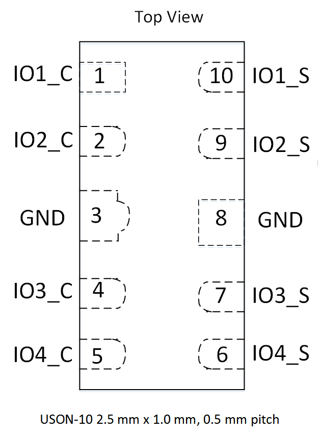
ESD224 Package_Outline_TopView.gif

Pin Functions

PIN TYPE DESCRIPTION
NAME NO.
GND 3 Ground Ground. Connect to ground. These pins are shorted internally.
GND 8
IO1_C 1 Connector Side I/O ESD protected channel to be connected to the connector
IO2_C 2
IO3_C 4
IO4_C 5
IO4_S 6 System Side I/O Pin corresponding to IO4_C To be connected to the system side
IO3_S 7 System Side I/O Pin corresponding to IO3_C
IO2_S 9 System Side I/O Pin corresponding to IO2_C
IO1_S 10 System Side I/O Pin corresponding to IO1_C