SLVSEB4A February 2018 – March 2018 ESD224
PRODUCTION DATA.
- 1 Features
- 2 Applications
- 3 Description
- 4 Revision History
- 5 Pin Configuration and Functions
- 6 Specifications
- 7 Parameter Measurement Setup
- 8 Detailed Description
- 9 Application and Implementation
- 10Power Supply Recommendations
- 11Layout
- 12Device and Documentation Support
- 13Mechanical, Packaging, and Orderable Information
Package Options
Mechanical Data (Package|Pins)
- DQA|10
Thermal pad, mechanical data (Package|Pins)
- DQA|10
Orderable Information
6.7 Typical Characteristics
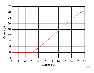 Figure 1. Positive TLP Curve, Connector side IO Pin to GND (tp=100ns)
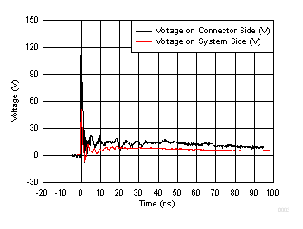 Figure 3. Clamping voltage waveform for +8kV IEC 61000-4-2 stress. See Figure 11 for details.
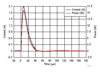 Figure 5. IEC 61000-4-5 Surge Waveform (tp=8/20 µs)
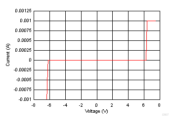 Figure 7. DC Voltage Sweep I-V Curve, IO Pin to GND
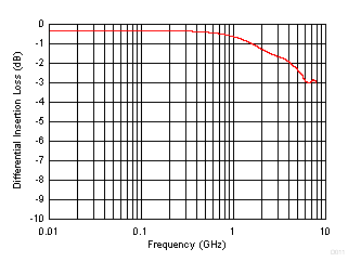 Figure 9. Differential Insertion Loss
 Figure 2. Negative TLP Curve, Connector side IO Pin to GND (Plotted as positive TLP from GND to IO, tp=100ns )
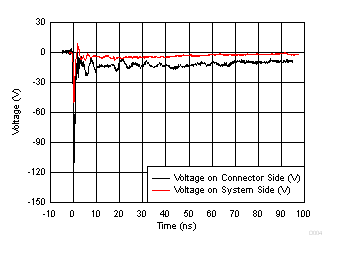 Figure 4. Clamping voltage waveform for -8kV IEC 61000-4-2 stress. See Figure 11 for details.
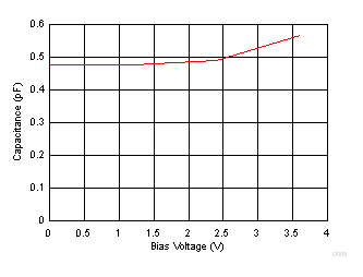 Figure 6. Capacitance vs. Bias Voltage at 25 degree Celsius
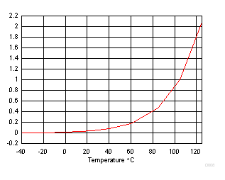 Figure 8. Leakage Current vs Temperature, IO Pin to GND, at 2.5 V Bias
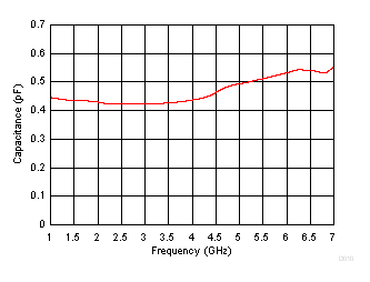 Figure 10. Capacitance vs Frequency