SLAS901C December 2016 – January 2021 HD3SS213
PRODUCTION DATA
- 1 Features
- 2 Applications
- 3 Description
- 4 Revision History
- 5 Pin Configuration and Functions
- 6 Specifications
- 7 Detailed Description
- 8 Application and Implementation
- 9 Layout
- 10Device and Documentation Support
- 11Mechanical, Packaging, and Orderable Information
Package Options
Mechanical Data (Package|Pins)
- ZXH|50
Thermal pad, mechanical data (Package|Pins)
Orderable Information
8.1 Application Information
Many interfaces require AC coupling between the source and sink. The 0402 capacitors are the preferred option to provide AC coupling, and the 0603 size capacitors also work. The 0805 size capacitors and C-packs must be avoided. When placing AC coupling capacitors symmetric placement is best. A capacitor value of 0.1 µF is best and the value must be match for the ± signal pair. There are several placement options for the AC coupling capacitors. Because the switch requires a bias voltage, the capacitors must only be placed on one side of the switch. If they are placed on both sides of the switch, a biasing voltage must be provided. A few placement options are shown below.
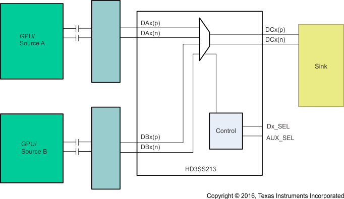
In Figure 8-1, the coupling capacitors are placed on the source pair. In this situation, the switch is biased by the sink.
 Figure 8-1 Source Biased by the Sink
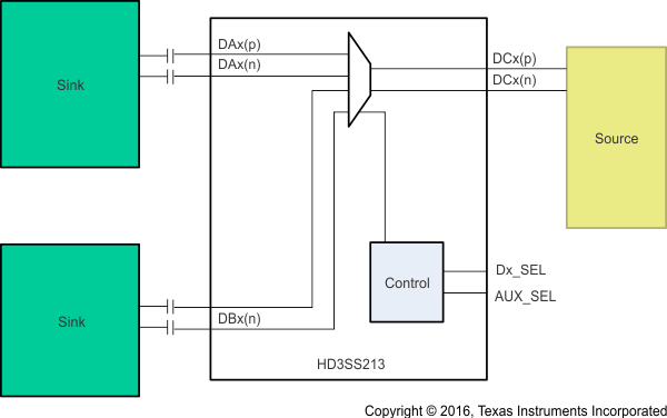
In Figure 8-2, the coupling capacitors are placed between the switch and Sink. In this situation, the switch is biased by the Source
 Figure 8-2 Switch Biased by the Source