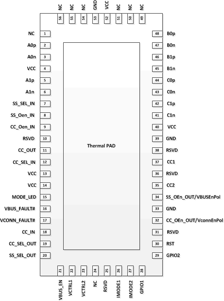
| A0p |
2 |
I/O |
Port A0, High Speed Positive Signal |
| A0n |
3 |
I/O |
Port A0, High Speed Negative Signal |
| A1p |
5 |
I/O |
Port A1, High Speed Positive Signal |
| A1n |
6 |
I/O |
Port A1, High Speed Negative Signal |
| B0p |
48 |
I/O |
Port B0, High Speed Positive Signal |
| B0n |
47 |
I/O |
Port B0, High Speed Negative Signal |
| B1p |
46 |
I/O |
Port B1, High Speed Positive Signal |
| B1n |
45 |
I/O |
Port B1, High Speed Negative Signal |
| C0p |
44 |
I/O |
Port C0, High Speed Positive Signal |
| C0n |
43 |
I/O |
Port C0, High Speed Negative Signal |
| C1p |
42 |
I/O |
Port C1, High Speed Positive Signal |
| C1n |
41 |
I/O |
Port C1, High Speed Negative Signal |
| CC_IN |
18 |
I/O |
Selected CC signal back to the device as input - connect to CC_OUT pin |
| CC_OUT |
11 |
I/O |
Selected CC signal as output - connect to CC_IN pin |
| CC_SEL_IN |
12 |
I |
CC Signal select pin input – Connect to CC_SEL_OUT |
| CC_SEL_OUT |
19 |
O |
CC Signal select pin output – Connect to CC_SEL_IN |
| CC_OEn_IN |
9 |
I |
Active Low CC MUX Enable input – connect to CC_OEn_OUT |
CC_OEn_OUT /
VconnEnPol |
32 |
I/O |
Active Low CC MUX Enable output – connect to CC_OEn. The pin is also sampled upon reset to set the polarity of the VCTRL1 and VCTRL2.
0 = VCTRL1/2 polarity is active high.
1 = VCTRL1/2 polarity is active low. |
| CC1 |
37 |
I/O |
USB Type-C configuration channel for position 1 |
| CC2 |
35 |
I/O |
USB Type-C configuration channel for position 2 |
| GND |
33 , 39, 53 |
G |
Ground |
| GPIO1 |
28 |
I/O |
GPIO or SCL for FW update |
| GPIO2 |
29 |
I/O |
GPIO or SDA for FW update |
IMODE1
IMODE2 |
26
27 |
I |
IMODE1 |
IMODE2 |
Current Mode |
| Low |
Low |
Default |
| Low |
High |
Mid (1.5 A) |
| High |
Low |
Reserved |
| High |
High |
High (3A) |
| MODE_LED |
15 |
O |
High when UFP attach detected |
| NC |
1, 24, 49, 50, 51, 54, 55, 56 |
|
Not connected |
| RST |
30 |
I |
CC Controller Reset |
| RSVD |
10, 25, 31, 36, 38 |
I/O |
Reserved |
| SS_OEn_IN |
8 |
I |
Active Low SS MUX Enable input – connect to SS_OEn_OUT |
SS_OEn_OUT /
VBUSEnPol |
34 |
I/O |
Active Low SS MUX Enable output – connect to SS_OEn_IN. The pin is also sampled upon reset to set the polarity of the VBUS_EN.
0 = VBUS_EN polarity is active high.
1 = VBUS_EN polarity is active low. |
| SS_SEL_IN |
7 |
I |
SS Port select pin input – Connect to SS_SEL_OUT |
| SS_SEL_OUT |
20 |
O |
SS Port select pin output – Connect to SS_SEL_IN |
| VBUS_EN |
21 |
O |
Polarity programmable via VBUSEnPol pin (pin 34). Driven low or high when UFP attach is detected. |
| VBUS_FAULT# |
16 |
I |
VBUS Fault signal in from VBUS Power switch. Active low. |
| VCC |
4 , 13, 14, 40, 52 |
P |
3.3V Power |
| VCONN_FAULT# |
17 |
I |
VCONN Fault signal in from VCONN switches. Active low. |
| VCTRL1 |
22 |
O |
Polarity programmable via VconnEnPol pin (pin 32). Driven low or high when active cable is detected. |
| VCTRL2 |
23 |
O |
Polarity programmable via VconnEnPol pin (pin 32). Driven low or high when active cable is detected. |
