SLASEB6 November 2015 HD3SS3411
PRODUCTION DATA.
- 1 Features
- 2 Applications
- 3 Description
- 4 Revision History
- 5 Pin Configuration and Functions
- 6 Specifications
- 7 Detailed Description
- 8 Application Information and Implementation
- 9 Power Supply Recommendations
- 10Layout
- 11Device and Documentation Support
- 12Mechanical, Packaging, and Orderable Information
Package Options
Mechanical Data (Package|Pins)
- RWA|14
Thermal pad, mechanical data (Package|Pins)
Orderable Information
7 Detailed Description
7.1 Overview
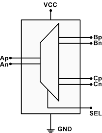
The HD3SS3411 is a high-speed bi-directional passive switch in mux or demux configurations. Based on control pin SEL, the device switches one differential channels between Port B or Port C to Port A.
The HD3SS3411 is a generic analog differential passive switch that can work for any high speed interface applications as long as it is biased at a common mode voltage range of 0 V to 2 V and has differential signaling with differential amplitude up to 1800 mVpp. The device employs an adaptive tracking that ensures the channel remains unchanged for entire common mode voltage range.
Table 1. MUX Pin Connections(1)
| PORT A CHANNEL | PORT B OR PORT C CHANNEL CONNECTED TO PORT A CHANNEL | |
|---|---|---|
| SEL = L | SEL = H | |
| Ap | Bp | Cp |
| An | Bn | Cn |
7.2 Functional Block Diagram

7.3 Feature Description
7.3.1 Output Enable and Power Savings
The HD3SS3411 has two power modes, normal operating mode and shutdown mode. During shutdown mode, the device consumes very-little current to save the maximum power. The OEn control pin is used to toggle between the two modes.
HD3SS3411 consumes < 2 mW of power when operational and has a shutdown mode exercisable by the OEn pin resulting < 20 µW.
7.4 Device Functional Modes
The OEn control pin selects the functional mode of HD3SS3411. To enter standby/shutdown mode, the OEn control pin is pulled high through a resistor and must remain high. For active/normal operation, the OEn control pin should be pulled low to GND or dynamically controlled to switch between H or L.
Table 2. Device Power Modes
| OEn | Device State | Signal Pins |
|---|---|---|
| L | Normal | Normal |
| H | Shutdown | Tri-stated |