SNAS658C May   2015  – December 2015 HDC1050

PRODUCTION DATA.  

  1. Features
  2. Applications
  3. Description
  4. Typical Application
  5. Revision History
  6. Pin Configuration and Functions
  7. Specifications
    1. 7.1 Absolute Maximum Ratings
    2. 7.2 ESD Ratings
    3. 7.3 Recommended Operating Conditions
    4. 7.4 Thermal Information
    5. 7.5 Electrical Characteristics
    6. 7.6 I2C Interface Electrical Characteristics
    7. 7.7 I2C Interface Timing Requirements
    8. 7.8 Typical Characteristics
  8. Detailed Description
    1. 8.1 Overview
    2. 8.2 Functional Block Diagram
    3. 8.3 Feature Description
      1. 8.3.1 Power Consumption
      2. 8.3.2 Voltage Supply Monitoring
      3. 8.3.3 Heater
    4. 8.4 Device Functional Modes
    5. 8.5 Programming
      1. 8.5.1 I2C Interface
        1. 8.5.1.1 Serial Bus Address
        2. 8.5.1.2 Read and Write Operations
        3. 8.5.1.3 Device Measurement Configuration
    6. 8.6 Register Map
      1. 8.6.1 Temperature Register
      2. 8.6.2 Humidity Register
      3. 8.6.3 Configuration Register
      4. 8.6.4 Serial Number Registers
      5. 8.6.5 Manufacturer ID Register
      6. 8.6.6 Device Register ID
  9. Application and Implementation
    1. 9.1 Application Information
    2. 9.2 Typical Application
      1. 9.2.1 Design Requirements
      2. 9.2.2 Detailed Design Procedure
      3. 9.2.3 Application Curve
    3. 9.3 Do's and Don'ts
      1. 9.3.1 Soldering
      2. 9.3.2 Hydration Procedure
      3. 9.3.3 Chemical Exposure and Sensor Protection
  10. 10Power Supply Recommendations
  11. 11Layout
    1. 11.1 Layout Guidelines
    2. 11.2 Layout Example
  12. 12Device and Documentation Support
    1. 12.1 Documentation Support
      1. 12.1.1 Related Documentation
    2. 12.2 Community Resources
    3. 12.3 Trademarks
    4. 12.4 Electrostatic Discharge Caution
    5. 12.5 Glossary
  13. 13Mechanical, Packaging, and Orderable Information

Package Options

Mechanical Data (Package|Pins)
Thermal pad, mechanical data (Package|Pins)
Orderable Information

11 Layout

11.1 Layout Guidelines

The Relative Humidity sensor element is located on the top side of the package.

It is recommended to isolate the sensor from the rest of the PCB by eliminating copper layers below the device (GND, VDD) and creating a slot into the PCB around the sensor to enhance thermal isolation.

11.2 Layout Example

The only component next to the device is the supply bypass capacitor. Since the relative humidity is dependent on the temperature, the HDC1050 should be positioned away from hot spots present on the board, such as a battery, display or micro-controller. Slots around the device can be used to reduce the thermal mass, for a quicker response to environmental changes. The DAP may be soldered to a floating pad on the board, but the board pad should NOT be connected to GND.
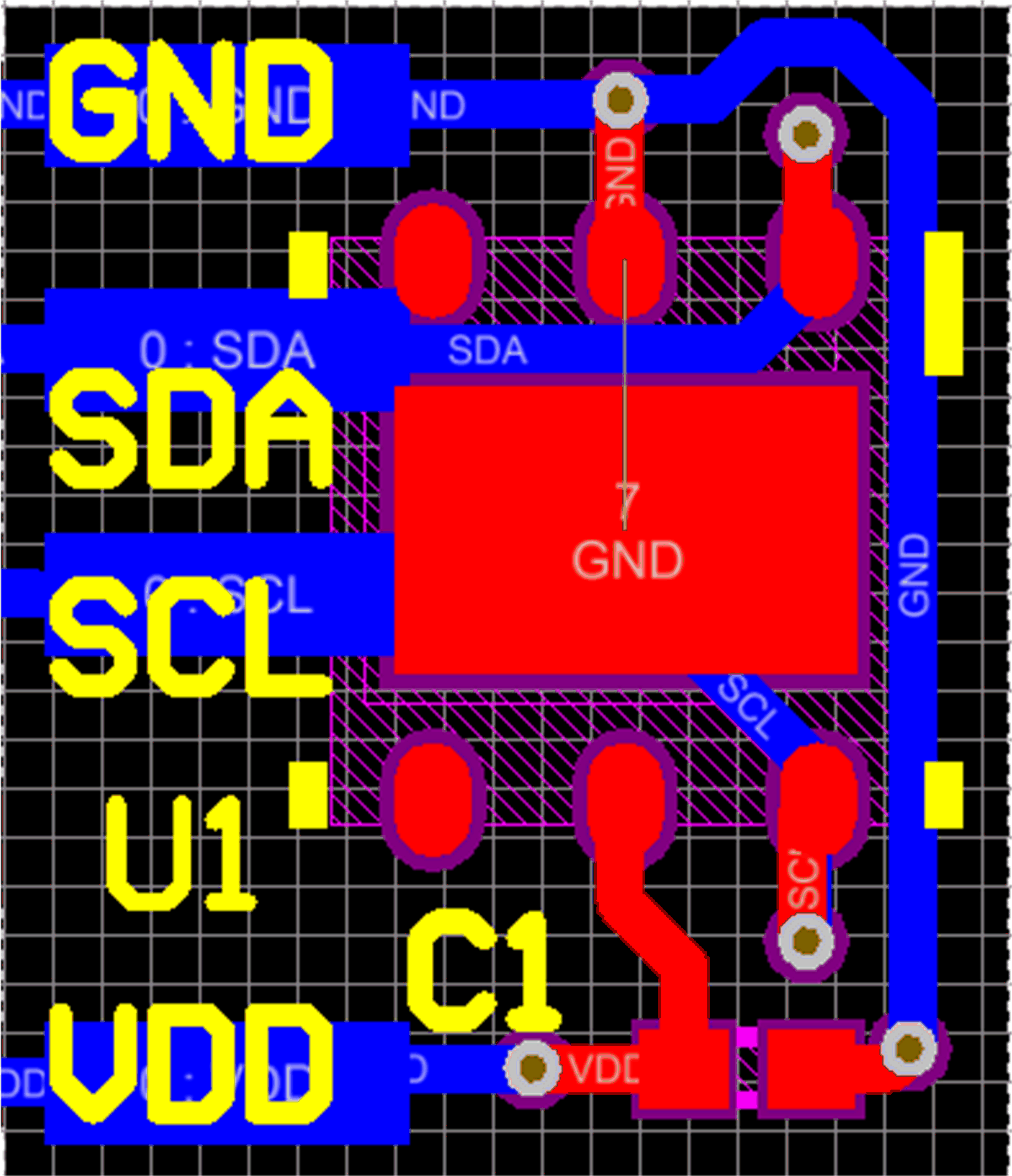
HDC1050 Layout_HDC1050.png Figure 17. Layout