SNAS658C May   2015  – December 2015 HDC1050

PRODUCTION DATA.  

  1. Features
  2. Applications
  3. Description
  4. Typical Application
  5. Revision History
  6. Pin Configuration and Functions
  7. Specifications
    1. 7.1 Absolute Maximum Ratings
    2. 7.2 ESD Ratings
    3. 7.3 Recommended Operating Conditions
    4. 7.4 Thermal Information
    5. 7.5 Electrical Characteristics
    6. 7.6 I2C Interface Electrical Characteristics
    7. 7.7 I2C Interface Timing Requirements
    8. 7.8 Typical Characteristics
  8. Detailed Description
    1. 8.1 Overview
    2. 8.2 Functional Block Diagram
    3. 8.3 Feature Description
      1. 8.3.1 Power Consumption
      2. 8.3.2 Voltage Supply Monitoring
      3. 8.3.3 Heater
    4. 8.4 Device Functional Modes
    5. 8.5 Programming
      1. 8.5.1 I2C Interface
        1. 8.5.1.1 Serial Bus Address
        2. 8.5.1.2 Read and Write Operations
        3. 8.5.1.3 Device Measurement Configuration
    6. 8.6 Register Map
      1. 8.6.1 Temperature Register
      2. 8.6.2 Humidity Register
      3. 8.6.3 Configuration Register
      4. 8.6.4 Serial Number Registers
      5. 8.6.5 Manufacturer ID Register
      6. 8.6.6 Device Register ID
  9. Application and Implementation
    1. 9.1 Application Information
    2. 9.2 Typical Application
      1. 9.2.1 Design Requirements
      2. 9.2.2 Detailed Design Procedure
      3. 9.2.3 Application Curve
    3. 9.3 Do's and Don'ts
      1. 9.3.1 Soldering
      2. 9.3.2 Hydration Procedure
      3. 9.3.3 Chemical Exposure and Sensor Protection
  10. 10Power Supply Recommendations
  11. 11Layout
    1. 11.1 Layout Guidelines
    2. 11.2 Layout Example
  12. 12Device and Documentation Support
    1. 12.1 Documentation Support
      1. 12.1.1 Related Documentation
    2. 12.2 Community Resources
    3. 12.3 Trademarks
    4. 12.4 Electrostatic Discharge Caution
    5. 12.5 Glossary
  13. 13Mechanical, Packaging, and Orderable Information

Package Options

Mechanical Data (Package|Pins)
Thermal pad, mechanical data (Package|Pins)
Orderable Information

6 Pin Configuration and Functions

DMB Package
6 Pin PWSON
Top View
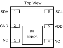
HDC1050 PINOUT.gif

Pin Functions

PIN I/O TYPE(1) DESCRIPTION
NAME NO.
SDA 1 I/O Serial data line for I2C, open-drain; requires a pull-up resistor to VDD
GND 2 G Ground
NC 3,4 - These pins may be left floating, or connected to GND
VDD 5 P Supply Voltage
SCL 6 I Serial clock line for I2C, open-drain; requires a pull-up resistor to VDD
DAP DAP G Die Attach Pad. Should be left floating. (On bottom of the device, not shown in the figure)
(1) P=Power, G=Ground, I=Input, O=Output