SBOS014A September 2000 – January 2024 INA114
PRODUCTION DATA
- 1
- 1 Features
- 2 Applications
- 3 Description
- 4 Pin Configuration and Functions
- 5 Specifications
- 6 Application and Implementation
- 7 Typical Applications
- 8 Device and Documentation Support
- 9 Revision History
- 10Mechanical, Packaging, and Orderable Information
Package Options
Refer to the PDF data sheet for device specific package drawings
Mechanical Data (Package|Pins)
- P|8
- DW|16
Thermal pad, mechanical data (Package|Pins)
- DW|16
Orderable Information
5.6 Typical Characteristics
at TA = +25°C, VS = ±15V, G = 1V/V (unless otherwise noted)
 Figure 5-1 Gain vs Frequency
 Figure 5-3 Input Common-mode Voltage
Range vs Output Voltage
 Figure 5-5 Negative Power Supply
Rejection vs Frequency
 Figure 5-7 Settling Time vs
Gain
 Figure 5-9 Input Bias and Input
Offset Current vs Temperature
 Figure 5-11 Input Bias Current vs
Common-Mode Input Voltage
 Figure 5-13 Slew Rate vs
Temperature
 Figure 5-15 Quiescent Current vs
Temperature
| RL = 2kΩ |

| G = 1 |

| G = 1000 |
 Figure 5-23 Input-Referred Noise,
0.1Hz to 10Hz
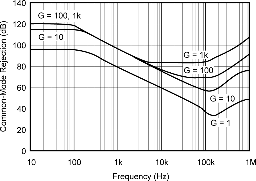
 Figure 5-2 Common-mode Rejection vs
Frequency
 Figure 5-4 Positive Power Supply
Rejection vs Frequency
 Figure 5-6 Input-Referred Noise
Voltage vs Frequency
 Figure 5-8 Offset Voltage Warm-up vs
Time
 Figure 5-10 Input Bias Current vs
Differential Input Voltage
 Figure 5-12 Maximum Output Swing vs
Frequency
 Figure 5-14 Output Current Limit vs
Temperature
 Figure 5-16 Quiescent Current and
Power Dissipation vs Power Supply Voltage
| RL = 2kΩ |

| G = 1 |

| G = 1000 |