SBOS501F January 2010 – February 2015 INA128-HT , INA129-HT
PRODUCTION DATA.
- 1 Features
- 2 Applications
- 3 Description
- 4 Simplified Schematic
- 5 Revision History
- 6 Pin Configuration and Functions
- 7 Specifications
- 8 Detailed Description
- 9 Application and Implementation
- 10Power Supply Recommendations
- 11Layout
- 12Device and Documentation Support
- 13Mechanical, Packaging, and Orderable Information
Package Options
Mechanical Data (Package|Pins)
Thermal pad, mechanical data (Package|Pins)
Orderable Information
9 Application and Implementation
NOTE
Information in the following applications sections is not part of the TI component specification, and TI does not warrant its accuracy or completeness. TI’s customers are responsible for determining suitability of components for their purposes. Customers should validate and test their design implementation to confirm system functionality.
9.1 Application Information
The INA12x measures small differential voltage with high common-mode voltage developed between the non-inverting and inverting input. The high-input voltage protection circuit in conjunction with high input impedance make the INA12x suitable for a wide range of applications. The ability to set the reference pin to adjust the functionality of the output signal offers additional flexibility that is practical for multiple configurations.
9.2 Typical Application
Figure 20 shows the basic connections required for operation of the INA128-HT and INA129-HT. Applications with noisy or high impedance power supplies may require decoupling capacitors close to the device pins as shown.
The output is referred to the output reference (Ref) pin that is normally grounded. This must be a low-impedance connection to assure good common-mode rejection. A resistance of 8 Ω in series with the Ref pin will cause a typical device to degrade.
 Figure 20. Basic Connections
9.2.1 Design Requirements
The device can be configured to monitor the input differential voltage when the gain of the input signal is set by the external resistor RG. The output signal references to the Ref pin. The most common application is where the output is referenced to ground when no input signal is present by connecting the Ref pin to ground, as Figure 20 shows. When the input signal increases, the output voltage at the OUT pin increases, too.
9.2.2 Detailed Design Procedure
9.2.2.1 Setting the Gain
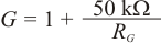
Gain is set by connecting a single external resistor, RG, between pins 1 and 8.
INA128-HT:
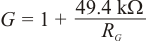
INA129-HT:
Commonly used gains and resistor values are shown in Figure 20.
The 50-kΩ term in Equation 1 (49.4-kΩ in Equation 2) comes from the sum of the two internal feedback resistors of A1 and A2. These on-chip metal film resistors are laser trimmed to accurate absolute values. The accuracy and temperature coefficient of these internal resistors are included in the gain accuracy and drift specifications of the INA128-HT and INA129-HT.
The stability and temperature drift of the external gain setting resistor, RG, also affects gain. The RG contribution to gain accuracy and drift can be directly inferred from Equation 2. Low resistor values required for high gain can make wiring resistance important. Sockets add to the wiring resistance which will contribute additional gain error (possibly an unstable gain error) in gains of approximately 100 or greater.
9.2.2.2 Dynamic Performance
Figure 2 shows that, despite its low quiescent current, the INA128-HT and INA129-HT achieve wide bandwidth, even at high gain. This is due to the current-feedback topology of the input stage circuitry. Settling time also remains excellent at high gain.
9.2.2.3 Offset Trimming
The INA128-HT and INA129-HT are laser trimmed for low offset voltage and offset voltage drift. Most applications require no external offset adjustment. Figure 21 shows an optional circuit for trimming the output offset voltage. The voltage applied to Ref terminal is summed with the output. The operational amplifier buffer provides low impedance at the Ref terminal to preserve good common-mode rejection.

9.2.2.4 Input Bias Current Return Path
The input impedances of the INA128-HT and INA129-HT are extremely high (approximately 1010 Ω). However, a path must be provided for the input bias current of both inputs. This input bias current is approximately ±50 nA. High input impedance means that this input bias current changes very little with varying input voltage.
Input circuitry must provide a path for this input bias current for proper operation. Figure 22 shows various provisions for an input bias current path. Without a bias current path, the inputs will float to a potential which exceeds the common-mode range, and the input amplifiers will saturate.
If the differential source resistance is low, the bias current return path can be connected to one input (see the thermocouple example in Figure 22). With higher source impedance, using two equal resistors provides a balanced input with possible advantages of lower input offset voltage due to bias current and better high-frequency common-mode rejection.
 Figure 22. Providing an Input Common-Mode Current Path
9.2.3 Application Curves

| G = 1, 10 | ||

| G = 1, 10 | ||

| G = 100, 1000 | ||

| G = 100, 1000 | ||