SBOS501F January 2010 – February 2015 INA128-HT , INA129-HT
PRODUCTION DATA.
- 1 Features
- 2 Applications
- 3 Description
- 4 Simplified Schematic
- 5 Revision History
- 6 Pin Configuration and Functions
- 7 Specifications
- 8 Detailed Description
- 9 Application and Implementation
- 10Power Supply Recommendations
- 11Layout
- 12Device and Documentation Support
- 13Mechanical, Packaging, and Orderable Information
Package Options
Mechanical Data (Package|Pins)
Thermal pad, mechanical data (Package|Pins)
Orderable Information
10 Power Supply Recommendations
The minimum power supply voltage for INA12x is ±2.25 V and the maximum power supply voltage is ±18 V. This minimum and maximum range covers a wide range of power supplies; but for optimum performance, ±15 V is recommended. TI recommends adding a bypass capacitor at the input to compensate for the layout and power supply source impedance.
10.1 Low Voltage Operation
The INA128-HT and INA129-HT can be operated on power supplies as low as ±2.25 V. Performance remains excellent with power supplies ranging from ±2.25 V to ±18 V. Most parameters vary only slightly throughout this supply voltage range.
Operation at very low supply voltage requires careful attention to assure that the input voltages remain within their linear range. Voltage swing requirements of internal nodes limit the input common-mode range with low power supply voltage. Figure 6 and Figure 7 show the range of linear operation for ±15 V, ±5 V, and ±2.5 V supplies.
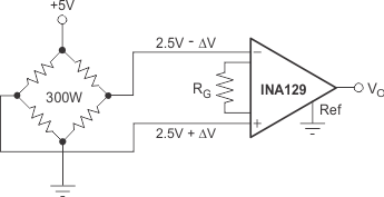 Figure 27. Bridge Amplifier
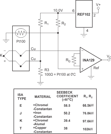
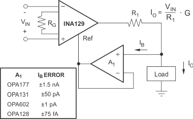 Figure 30. Differential Voltage-to-Current Converter
