SBOS059A November 1996 – February 2024 INA132
PRODUCTION DATA
- 1
- 1Features
- 2Applications
- 3Description
- 4Pin Configuration and Functions
- 5Specifications
- 6Application and Implementation
- 7Device and Documentation Support
- 8Revision History
- 9Mechanical, Packaging, and Orderable Information
Package Options
Refer to the PDF data sheet for device specific package drawings
Mechanical Data (Package|Pins)
- D|8
Thermal pad, mechanical data (Package|Pins)
Orderable Information
6.1 Applications Information
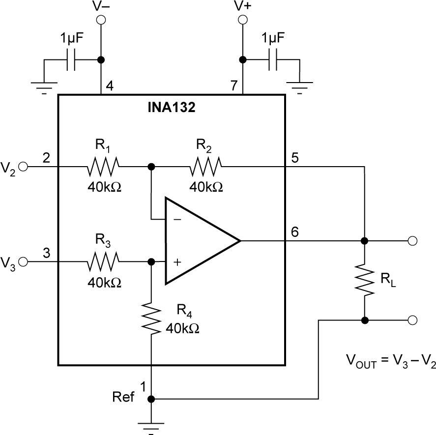
Figure 6-1 shows the basic connections required for operation of the INA132. Connect power-supply bypass capacitors close to the device pins.
The differential input signal is connected to pins 2 and 3 as shown. Ensure that the source impedances connected to the inputs are nearly equal to maintain good common-mode rejection. An 8Ω mismatch in source impedance degrades the common-mode rejection of a typical device to approximately 80dB. Gain accuracy is also slightly affected. If the source has a known impedance mismatch, use an additional resistor in series with one input to preserve good common-mode rejection.
Do not interchange pins 1 and 3 or pins 2 and 5, even though nominal resistor values are equal. These resistors are laser trimmed for precise resistor ratios to achieve accurate gain and highest CMR. Interchanging these pins does not provide specified performance. Sense measurements at the load, as in Figure 6-1.
 Figure 6-1 Basic Power Supply and Signal
Connections