SBOS472B March 2009 – June 2016 INA148-Q1
PRODUCTION DATA.
- 1 Features
- 2 Applications
- 3 Description
- 4 Revision History
- 5 Pin Configuration and Functions
- 6 Specifications
- 7 Detailed Description
- 8 Application and Implementation
- 9 Power Supply Recommendations
- 10Layout
- 11Device and Documentation Support
- 12Mechanical, Packaging, and Orderable Information
Package Options
Refer to the PDF data sheet for device specific package drawings
Mechanical Data (Package|Pins)
- D|8
Thermal pad, mechanical data (Package|Pins)
Orderable Information
7 Detailed Description
7.1 Overview
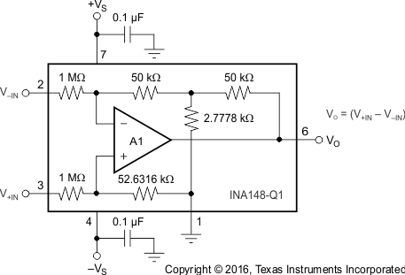
The INA148-Q1 is a unity-gain difference amplifier with a high common-mode input voltage range. To achieve its high common-mode voltage range, the INA148-Q1 features a precision, laser-trimmed, thin-film resistor network with a 20:1 input voltage divider ratio. High input voltages are thereby reduced in amplitude, delivering input voltages to the op amp that are within its linear operating range. A Tee network in the op amp feedback network places the amplifier in a gain of 20 V/V, restoring the overall circuit gain to unity (1 V/V).
External voltages can be summed into the amplifier's output by using the REF pin, making the differential amplifier a highly versatile design tool. Voltages on the REF pin also influence the INA148-Q1's common-mode voltage range.
In accordance with good engineering practice for linear integrated circuits, the INA148-Q1's power-supply bypass capacitors must be connected as close to the supply pins (V+ and V–) as practical. TI recommends ceramic or tantalum capacitors for use as bypass capacitors.
The input impedances are unusually high for a difference amplifier and this must be considered when routing input signal traces on a PCB. Avoid placing digital signal traces near the difference amplifier's input traces to minimize noise pickup.
7.2 Functional Block Diagram

7.3 Feature Description
7.3.1 Operating Voltage
The INA148-Q1 is specified for ±15-V and ±5-V dual supplies and 5-V single supplies. The INA148-Q1 can be operated with single or dual supplies with excellent performance.
The INA148-Q1 is fully characterized for supply voltages from ±1.35 V to ±18 V and over temperatures of –40°C to 125°C. Parameters that vary significantly with operating voltage, load conditions, or temperature are shown in Typical Characteristics.
7.3.2 Gain Equation
An internal on-chip resistor network sets the overall differential gain of the INA148-Q1 to precisely 1 V/V. Equation 1 shows the output.
7.3.3 Common-Mode Range
The 20:1 input resistor ratio of the INA148-Q1 provides an input common-mode range that extends well beyond its power supply rails.
The exact input voltage range depends on the amplifier's power-supply voltage and the voltage applied to the REF pin. See Typical Applications for typical input voltage ranges at different power supply voltages.
7.3.4 Offset Trim
The INA148-Q1 is laser-trimmed for low offset voltage and drift. Most applications require no external offset adjustment.
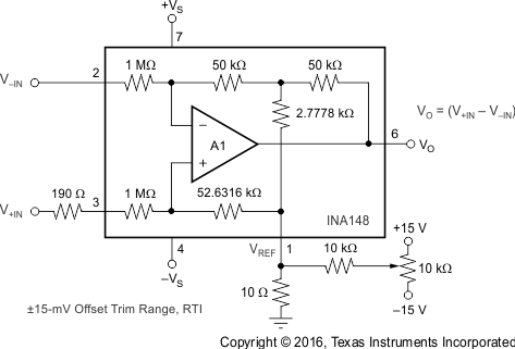
Because a voltage applied to the reference (REF) pin is summed directly into the amplifier's output signal, this technique can be used to null the amplifier's input offset voltage. Figure 21 shows an optional circuit for trimming the offset voltage.
 Figure 21. Optional Offset Trim Circuit
To maintain high common-mode rejection (CMR), the source impedance of any signal applied to the REF pin must be very low (≤5 Ω).
A source impedance of only 10 Ω at the REF pin reduces the INA148-Q1's CMR to approximately 74 dB. High CMR can be restored if a resistor is added in series with the amplifier's positive input pin. This resistor must be 19 times the source impedance that drives the REF pin. For example, if there is a source impedance of 10 Ω to the REF pin, a 190-Ω resistor must be added in series with the +IN pin.
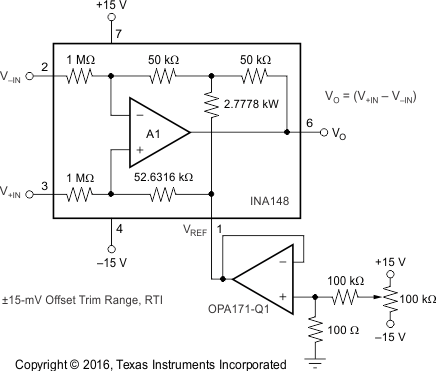
Preferably, the offset trim voltage applied to the REF pin must be buffered with an amplifier such as an OPA171-Q1 (see Figure 22). In this case, the op amp output impedance is low enough that no external resistor is needed to maintain the INA148-Q1's excellent CMR.
 Figure 22. Preferred Offset Trim Circuit
7.3.5 Input Impedance
The input resistor network determines the impedance of each of the INA148-Q1 inputs. The impedance is approximately 1 MΩ. Unlike an instrumentation amplifier, signal source impedances at the two input pins must be nearly equal to maintain good common-mode rejection.
A mismatch between the two input source impedances causes a differential amplifier's common-mode rejection to be degraded. With a source impedance imbalance of only 500 Ω, CMR can fall to approximately 66 dB.
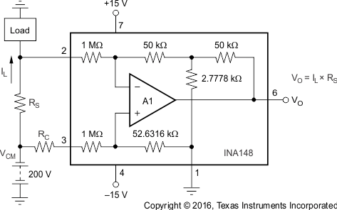
Figure 23 shows a common application, measuring power supply current through a shunt resistor (RS). A shunt resistor creates an unbalanced source resistance condition that can degrade a differential amplifier's common-mode rejection.
 Figure 23. Shunt-Resistor Current Measurement Circuit
Unless the shunt resistor is less than approximately 100 Ω, TI recommends an additional equal compensating resistor (RC) to maintain input balance and high CMR.
Source impedances (or shunts) greater than 5 kΩ are not recommended, even if they are perfectly compensated. This is because the internal resistor network is laser-trimmed for accurate voltage divider ratios, but not necessarily to absolute values. Input resistors are shown as 1 MΩ; however, this is only their nominal value.
In practice, the input resistors' absolute values may vary by as much as 30%. The two input resistors match to about 5%, so adding compensating resistors greater than 5 kΩ can cause a serious mismatch in the resulting resistor network voltage divider ratios, thus degrading CMR.
TI recommends not attempting to extend the INA148-Q1 input voltage range by adding external resistors for the reasons described in the previous paragraph. CMR suffers serious degradation unless the resistors are carefully trimmed for CMR and gain. This is an iterative adjustment and can be tedious and time consuming.
7.4 Device Functional Modes
The INA148-Q1 is a unity-gain, differential to single-ended amplifier that can reject high common-mode signals up to ±200 V with ±15-V supply voltage. This high common-mode rejection is achieved by internal trimmed resistive divider network. The resistive network provides an attenuation factor of 20:1.
Equation 2 shows the transfer function output to input.