SBOS472B March 2009 – June 2016 INA148-Q1
PRODUCTION DATA.
- 1 Features
- 2 Applications
- 3 Description
- 4 Revision History
- 5 Pin Configuration and Functions
- 6 Specifications
- 7 Detailed Description
- 8 Application and Implementation
- 9 Power Supply Recommendations
- 10Layout
- 11Device and Documentation Support
- 12Mechanical, Packaging, and Orderable Information
Package Options
Refer to the PDF data sheet for device specific package drawings
Mechanical Data (Package|Pins)
- D|8
Thermal pad, mechanical data (Package|Pins)
Orderable Information
6 Specifications
6.1 Absolute Maximum Ratings
over operating free-air temperature range (unless otherwise noted)(1)| MIN | MAX | UNIT | ||
|---|---|---|---|---|
| Supply voltage | V+ to V– | 36 | V | |
| Input voltage | Continuous | ±200 | V | |
| Peak (0.1 s) | ±500 | |||
| Short circuit to ground duration | Continuous | |||
| Package thermal impedance, junction to free air | 97.1 | °C/W | ||
| Operating free-air temperature | –40 | 125 | °C | |
| Maximum operating virtual-junction temperature | 150 | °C | ||
| Lead temperature (soldering, 10 s) | 300 | °C | ||
| Storage temperature, Tstg | –65 | 150 | °C | |
(1) Stresses beyond those listed under Absolute Maximum Ratings may cause permanent damage to the device. These are stress ratings only, which do not imply functional operation of the device at these or any other conditions beyond those indicated under Recommended Operating Conditions. Exposure to absolute-maximum-rated conditions for extended periods may affect device reliability.
6.2 ESD Ratings
| VALUE | UNIT | |||
|---|---|---|---|---|
| V(ESD) | Electrostatic discharge | Human-body model (HBM), per AEC Q100-002(1) | ±1500 | V |
| Charged-device model (CDM), per AEC Q100-011 | ±2000 | |||
| Machine model | ±150 | |||
(1) AEC Q100-002 indicates that HBM stressing shall be in accordance with the ANSI/ESDA/JEDEC JS-001 specification.
6.3 Recommended Operating Conditions
over operating free-air temperature range (unless otherwise noted)| MIN | MAX | UNIT | |||
|---|---|---|---|---|---|
| VS | Supply voltage | Single supply | 2.7 | 36 | V |
| Dual supply | ±1.35 | ±18 | |||
| TA | Operating free-air temperature | –40 | 125 | °C | |
6.4 Thermal Information
| THERMAL METRIC(1) | INA148-Q1 | UNIT | |
|---|---|---|---|
| D (SOIC) | |||
| 8 PINS | |||
| RθJA | Junction-to-ambient thermal resistance | 100.6 | °C/W |
| RθJC(top) | Junction-to-case (top) thermal resistance | 44.9 | °C/W |
| RθJB | Junction-to-board thermal resistance | 42.2 | °C/W |
| ψJT | Junction-to-top characterization parameter | 6.3 | °C/W |
| ψJB | Junction-to-board characterization parameter | 41.5 | °C/W |
(1) For more information about traditional and new thermal metrics, see the Semiconductor and IC Package Thermal Metrics application report, SPRA953.
6.5 Electrical Characteristics Dual Supply
VS = ±5 V to ±15 V (dual supply), RL = 10 kΩ to ground, VREF = 0 V, TA = 25°C (unless otherwise noted)| PARAMETER | TEST CONDITIONS | MIN | TYP | MAX | UNIT | ||
|---|---|---|---|---|---|---|---|
| VOS | Input offset voltage(1)(2) | VCM = 0 V | VS = ±15 V | ±1 | ±5 | mV | |
| VS = ±5 V | ±1 | ±5 | |||||
| ΔVOS/ΔT | Input offset voltage drift(1) | TA = –40°C to 125°C | ±10 | μV/°C | |||
| PSRR | Power supply ripple rejection(1) | VS = ±1.35 V to ±18 V, VCM = 0 V | ±50 | ±400 | μV/V | ||
| VCM | Common-mode voltage range | V+IN – V–IN = 0 | VS = ±15 V | –200 | 200 | V | |
| VS = ±5 V | –100 | 80 | |||||
| CMRR | Common-mode rejection ratio | VS = ±15 V, VCM = –200 V to 200 V, RS = 0 Ω | 70 | 86 | dB | ||
| VS = ±5 V, VCM = –100 V to 80 V, RS = 0 Ω | 70 | 86 | |||||
| Differential input impedance | 2 | MΩ | |||||
| Common-mode input impedance | 1 | MΩ | |||||
| Vn | Voltage noise(1)(3) | f = 0.1 Hz to 10 Hz | 17 | μVp-p | |||
| Voltage noise density(1)(3) | f = 1 kHz | 880 | nV/√Hz | ||||
| Initial gain(1) | 1 | V/V | |||||
| Gain error | VO = (V– + 0.5) to (V+ – 1.5) | ±0.01% | ±0.075% | ||||
| Gain error over temperature | ±3 | ±10 | ppm/°C | ||||
| Gain nonlinearity | VO = (V– + 0.5) to (V+ – 1.5) | VS = ±15 V | ±0.001 | ±0.002 | %FSR | ||
| VS = ±5 V | ±0.001 | ||||||
| Small-signal bandwidth frequency response | 100 | kHz | |||||
| SR | Slew rate | 1 | V/μs | ||||
| ts | Settling time | VS = ±15 V, 10-V step | 0.1% | 21 | μs | ||
| 0.01% | 25 | ||||||
| VS = ±5 V, 6-V step | 0.1% | 21 | |||||
| 0.01% | 25 | ||||||
| Overload recovery | 50% input overload | 24 | μs | ||||
| VO | Output voltage | RL = 100 kΩ | V– + 0.25 | V+ – 1 | V | ||
| RL = 10 kΩ | V– + 0.5 | V+ – 1.5 | |||||
| IO | Output current | Short-circuit current, continuous to common | ±13 | mA | |||
| CL | Load capacitance | Stable operation | 10 | nF | |||
| IS | Supply current | VIN = 0, IO = 0 | ±260 | ±300 | μA | ||
(1) Overall difference amplifier configuration. Referred to input pins (V+IN and V–IN ), gain = 1 V/V.
(2) Includes effects of amplifier's input bias and offset currents.
(3) Includes effects of input current noise and thermal noise contribution of resistor network.
6.6 Electrical Characteristics Single Supply
VS = 5 V (single supply), RL = 10 kΩ to VS / 2, VREF = VS / 2, TA = 25°C (unless otherwise noted)| PARAMETER | TEST CONDITIONS | MIN | TYP | MAX | UNIT | ||
|---|---|---|---|---|---|---|---|
| VOS | Input offset voltage(1)(2) | VCM = VS / 2 | ±1 | ±5 | mV | ||
| ΔVOS/ΔT | Input offset voltage drift(1) | TA = –40°C to 125°C | ±10 | μV/°C | |||
| PSRR | Power supply ripple rejection(1) | VS = 2.7 V to 36 V, VCM = VS / 2 | ±50 | ±400 | μV/V | ||
| VCM | Common-mode voltage range | V+IN – V–IN = 0 | VREF = 0.25 V | –4 | 75 | V | |
| VREF = VS / 2 | –47.5 | 32.5 | |||||
| CMRR | Common-mode rejection ratio | VCM = –47.5 V to 32.5 V, RS = 0 Ω | 70 | 86 | dB | ||
| Differential input impedance | 2 | MΩ | |||||
| Common-mode input impedance | 1 | MΩ | |||||
| Vn | Voltage noise(1)(3) | f = 0.1 Hz to 10 Hz | 17 | μVp-p | |||
| Voltage noise density(1)(3) | f = 1 kHz | 880 | nV/√Hz | ||||
| Initial gain(1) | 1 | V/V | |||||
| Gain error | VO = 0.5 V to 3.5 V | ±0.01% | ±0.075% | ||||
| Gain error over temperature | ±3 | ±10 | ppm/°C | ||||
| Gain nonlinearity | VO = 0.5 V to 3.5 V | ±0.001 | %FSR | ||||
| Small-signal bandwidth | 100 | kHz | |||||
| SR | Slew rate | 1 | V/μs | ||||
| ts | Settling time | VS = 5 V, 3-V step | 0.1% | 21 | μs | ||
| 0.01% | 25 | ||||||
| Overload recovery | 50% input overload | 13 | μs | ||||
| VO | Output voltage | RL = 100 kΩ | V– + 0.25 | V+ – 1 | V | ||
| RL = 10 kΩ | V– + 0.5 | V+ – 1.5 | |||||
| IO | Output current | Short-circuit current, continuous to common | ±8 | mA | |||
| CL | Load capacitance | Stable operation | 10 | nF | |||
| IQ | Quiescent current | VIN = 0, IO = 0 | 260 | 300 | μA | ||
(1) Overall difference amplifier configuration. Referred to input pins (V+IN and V–IN ), gain = 1 V/V.
(2) Includes effects of amplifier's input bias and offset currents.
(3) Includes effects of input current noise and thermal noise contribution of resistor network.
6.7 Typical Characteristics
VS = ±15 V, RL = 10 kΩ to common, VREF = 0 V, TA = 25°C (unless otherwise noted)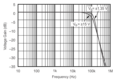 Figure 1. Gain vs Frequency
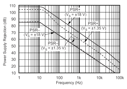 Figure 3. Power Supply Rejection vs Frequency
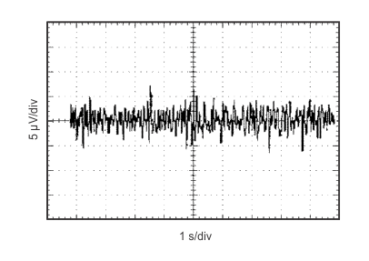
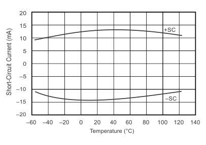 Figure 7. Short-Circuit Current vs Temperature
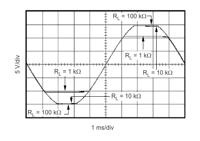
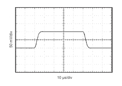
| RL = 10 kΩ | CL = 10 pF |
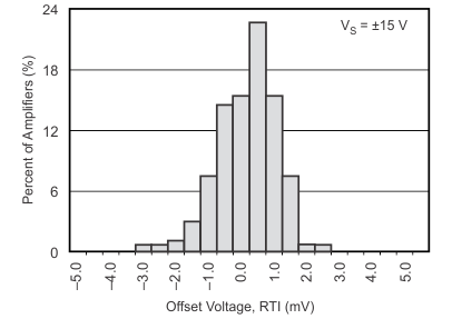 Figure 13. Offset Voltage Production Distribution
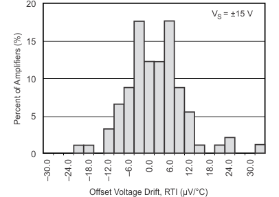 Figure 15. Offset Voltage Drift Production Distribution
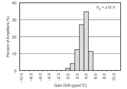 Figure 17. Gain Drift Production Distribution
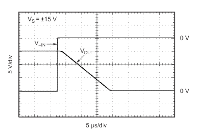 Figure 19. Inverting Input 50% Overload Recovery Time
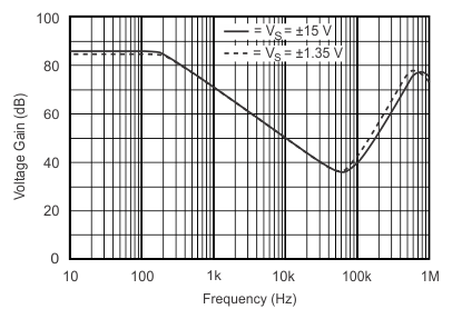 Figure 2. Common-Mode Rejection vs Frequency
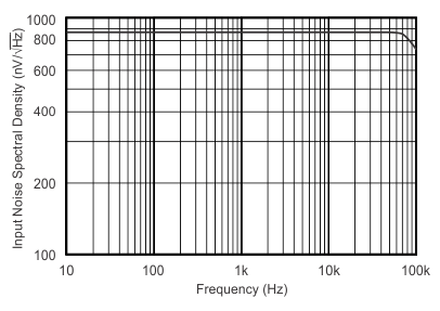 Figure 4. Input Voltage Noise Spectral Density
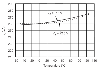 Figure 6. Quiescent Current vs Temperature
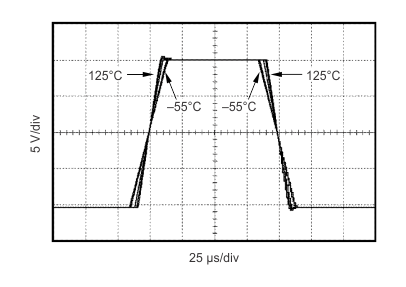 Figure 8. Large-Signal Step Response vs Temperature
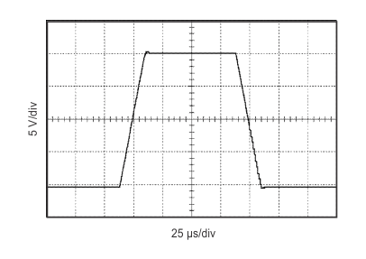
| RL = 10 kΩ | CL = 10 pF |
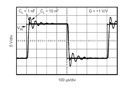
| CL = 1 nF and 10 nF |
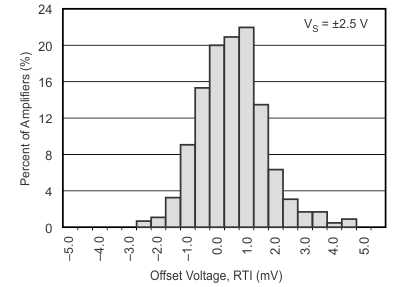 Figure 14. Offset Voltage Production Distribution
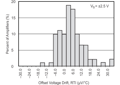 Figure 16. Offset Voltage Drift Production Distribution
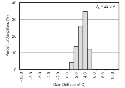 Figure 18. Gain Drift Production Distribution
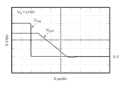 Figure 20. Noninverting Input 50% Overload Recovery Time