SBOS859B March   2018  – July 2018 INA1620

PRODUCTION DATA.  

  1. Features
  2. Applications
  3. Description
    1.     Device Images
      1.      INA1620 Simplified Internal Schematic
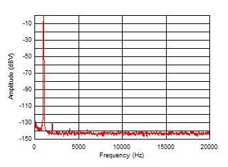
      2.      FFT: 1 kHz, 32-Ω Load, 50 mW
  4. Revision History
  5. Pin Configuration and Functions
    1.     Pin Functions
  6. Specifications
    1. 6.1 Absolute Maximum Ratings
    2. 6.2 ESD Ratings
    3. 6.3 Recommended Operating Conditions
    4. 6.4 Thermal Information
    5. 6.5 Electrical Characteristics:
    6. 6.6 Typical Characteristics
  7. Detailed Description
    1. 7.1 Overview
    2. 7.2 Functional Block Diagram
    3. 7.3 Feature Description
      1. 7.3.1 Matched Thin-Film Resistor Pairs
      2. 7.3.2 Power Dissipation
      3. 7.3.3 Thermal Shutdown
      4. 7.3.4 EN Pin
      5. 7.3.5 GND Pin
      6. 7.3.6 Input Protection
    4. 7.4 Device Functional Modes
      1. 7.4.1 Shutdown Mode
      2. 7.4.2 Output Transients During Power Up and Power Down
  8. Application and Implementation
    1. 8.1 Application Information
      1. 8.1.1 Noise Performance
      2. 8.1.2 Resistor Tolerance
      3. 8.1.3 EMI Rejection
      4. 8.1.4 EMIRR +IN Test Configuration
    2. 8.2 Typical Application
      1. 8.2.1 Design Requirements
      2. 8.2.2 Detailed Design Procedure
      3. 8.2.3 Application Curves
    3. 8.3 Other Application Examples
      1. 8.3.1 Preamplifier for Professional Microphones
  9. Power Supply Recommendations
  10. 10Layout
    1. 10.1 Layout Guidelines
    2. 10.2 Layout Example
  11. 11Device and Documentation Support
    1. 11.1 Device Support
      1. 11.1.1 Development Support
        1. 11.1.1.1 TINA-TI (Free Software Download)
        2. 11.1.1.2 TI Precision Designs
    2. 11.2 Documentation Support
      1. 11.2.1 Related Documentation
    3. 11.3 Receiving Notification of Documentation Updates
    4. 11.4 Community Resources
    5. 11.5 Trademarks
    6. 11.6 Electrostatic Discharge Caution
    7. 11.7 Glossary
  12. 12Mechanical, Packaging, and Orderable Information

Package Options

Mechanical Data (Package|Pins)
Thermal pad, mechanical data (Package|Pins)
Orderable Information

Application Curves

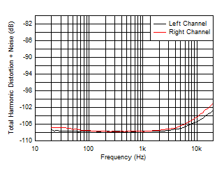
Figure 57 shows the maximum output voltage achievable for a 32-Ω load before the onset of clipping (±5-V supplies), indicated by a sharp increase in distortion. As more current is delivered by the output transistors of an amplifier, additional distortion is produced. At low frequencies, this distortion is corrected by the feedback loop of the amplifier. However, as the loop gain of the amplifier begins to decline at high frequencies, the overall distortion begins to climb. The unique output stage design of the INA1620 greatly reduces the additional distortion at high frequency when delivering large currents, as shown in Figure 58. High-ordered harmonics (above the 2nd and 3rd) are also kept to a minimal level at high output powers, as shown in Figure 59.
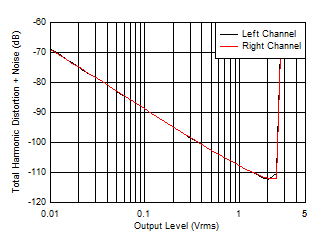
INA1620 THDN_vs_level_32_ohm.gif
22.4-kHz measurement bandwidth
Figure 57. THD+N vs Output Voltage for a 32-Ω Load
INA1620 FFT_Left_Channel_32_ohm.gif
1 kHz, 32-Ω load, 1 VRMS
Figure 59. Output Spectrum
INA1620 THDN_vs_Frequency_32_ohm.gif
90-kHz measurement bandwidth, 1-VRMS output
Figure 58. THD+N vs Frequency for a 32-Ω Load