SBOS366E August   2006  – January 2021 INA193A-Q1 , INA194A-Q1 , INA195A-Q1 , INA196A-Q1 , INA197A-Q1 , INA198A-Q1

PRODUCTION DATA  

  1. Features
  2. Applications
  3. Description
  4. Revision History
  5. Pin Configuration and Functions
  6. Specifications
    1. 6.1 Absolute Maximum Ratings
    2. 6.2 ESD Ratings
    3. 6.3 Recommended Operating Conditions
    4. 6.4 Thermal Information
    5. 6.5 Electrical Characteristics
    6. 6.6 Typical Characteristics
  7. Detailed Description
    1. 7.1 Overview
    2. 7.2 Functional Block Diagram
    3. 7.3 Feature Description
      1. 7.3.1 Basic Connection
      2. 7.3.2 Selecting RS
      3. 7.3.3 Inside the INA19xA
      4. 7.3.4 Power Supply
    4. 7.4 Device Functional Modes
      1. 7.4.1 Input Filtering
      2. 7.4.2 Accuracy Variations as a Result Of VSENSE and Common Mode Voltage
        1. 7.4.2.1 Normal Case 1: VSENSE ≥ 20 mV, VCM ≥ VS
        2. 7.4.2.2 Normal Case 2: VSENSE ≥ 20 mV, VCM < VS
        3. 7.4.2.3 Low VSENSE Case 1: VSENSE < 20 mV, –16 V ≤ VCM < 0; and Low VSENSE Case 3: VSENSE < 20 mV, VS < VCM ≤ 80 V
        4. 7.4.2.4 Low VSENSE Case 2: VSENSE < 20 mV, 0 V ≤ VCM ≤ VS
      3. 7.4.3 Shutdown
      4. 7.4.4 Transient Protection
      5. 7.4.5 Output Voltage Range
  8. Application and Implementation
    1. 8.1 Application Information
    2. 8.2 Typical Application
      1. 8.2.1 Design Requirements
      2. 8.2.2 Detailed Design Procedure
      3. 8.2.3 Application Curve
  9. Power Supply Recommendations
  10. 10Layout
    1. 10.1 Layout Guidelines
      1. 10.1.1 RFI/EMI
    2. 10.2 Layout Example
  11. 11Device and Documentation Support
    1. 11.1 Receiving Notification of Documentation Updates
    2. 11.2 Support Resources
    3. 11.3 Trademarks
    4. 11.4 Electrostatic Discharge Caution
    5. 11.5 Glossary
  12. 12Mechanical, Packaging, and Orderable Information

Package Options

Mechanical Data (Package|Pins)
Thermal pad, mechanical data (Package|Pins)
Orderable Information

Normal Case 1: VSENSE ≥ 20 mV, VCM ≥ VS

This region of operation provides the highest accuracy. Here, the input offset voltage is characterized and measured using a two-step method. First, the gain is determined by (Equation 2).
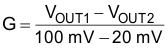
Equation 2. GUID-14DC5161-F9E7-4CCC-A8E4-A4510A71C610-low.gif

where

  • VOUT1 = Output voltage with VSENSE = 100 mV
  • VOUT2 = Output voltage with VSENSE = 20 mV

The offset voltage is then measured at VSENSE = 100 mV and referred to the input (RTI) of the current shunt monitor, as shown in (Equation 3).

Equation 3. GUID-DBAECD0C-657D-45A0-93D8-3421FC0E278F-low.gif

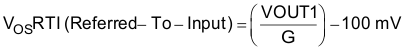
In Section 6.6, the Output Error vs Common Mode Voltage curve shows the highest accuracy for the this region of operation. In this plot, VS = 12 V; for VCM ≥ 12 V, the output error is at its minimum. This case is also used to create the VSENSE ≥ 20 mV output specifications in the Electrical Characteristics table.