SBOS539A December 2010 – April 2016 INA203-Q1
PRODUCTION DATA.
- 1 Features
- 2 Applications
- 3 Description
- 4 Revision History
- 5 Device Comparison Table
- 6 Pin Configuration and Functions
-
7 Specifications
- 7.1 Absolute Maximum Ratings
- 7.2 ESD Ratings
- 7.3 Recommended Operating Conditions
- 7.4 Thermal Information
- 7.5 Electrical Characteristics: Current-Shunt Monitor
- 7.6 Electrical Characteristics: Comparator
- 7.7 Electrical Characteristics: Reference
- 7.8 Electrical Characteristics: General
- 7.9 Typical Characteristics
- 8 Detailed Description
- 9 Application and Implementation
- 10Power Supply Recommendations
- 11Layout
- 12Device and Documentation Support
- 13Mechanical, Packaging, and Orderable Information
Package Options
Mechanical Data (Package|Pins)
- PW|14
Thermal pad, mechanical data (Package|Pins)
Orderable Information
11 Layout
11.1 Layout Guidelines
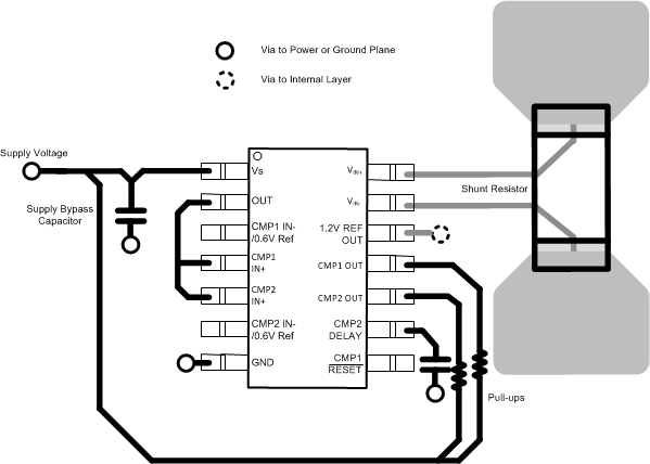
- Connect the input pins to the sensing resistor using a Kelvin or 4-wire connection. This connection technique ensures that only the current-sensing resistor impedance is detected between the input pins. Poor routing of the current-sensing resistor commonly results in additional resistance present between the input pins. Given the very low ohmic value of the current resistor, any additional high-current carrying impedance can cause significant measurement errors.
- The power-supply bypass capacitor should be placed as closely as possible to the supply and ground pins. TI recommends the value of this bypass capacitor is 0.1 μF. Additional decoupling capacitance can be added to compensate for noisy or high-impedance power supplies.
11.2 Layout Example
 Figure 38. Layout Recommendation