SLYS018E April 2018 – February 2024 INA181-Q1 , INA2181-Q1 , INA4181-Q1
PRODUCTION DATA
- 1
- 1 Features
- 2 Applications
- 3 Description
- 4 Device Comparison
- 5 Pin Configuration and Functions
- 6 Specifications
- 7 Detailed Description
- 8 Application and Implementation
- 9 Device and Documentation Support
- 10Revision History
- 11Mechanical, Packaging, and Orderable Information
Package Options
Refer to the PDF data sheet for device specific package drawings
Mechanical Data (Package|Pins)
- DGS|10
Thermal pad, mechanical data (Package|Pins)
Orderable Information
8.1.5 Detecting Leakage Currents
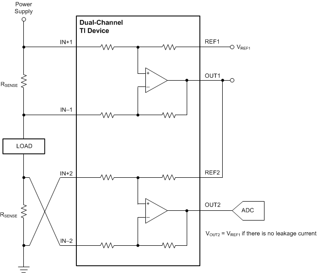
Occasionally, the need arises to confirm that the current going into a load is identical to the current coming out of a load; typically, as part of diagnostic testing or fault detection. This situation requires precision current differencing, which is the same as summing, except that the two amplifiers have the inputs connected opposite of each other. To correctly detect leakage currents, the values for the current sense resistor RSENSE must be the same for all channels. Provide an external reference voltage to the REF1 input to allow bidirectional leakage current detection.
If the current into a load is equal to the current out of the load, then the voltage at OUT2 is the same as the applied voltage to REF1. To enable accurate differences between the two currents, a reference voltage must be applied. The reference voltage prevents the output of the device from being driven to ground, and also enables detection if the current into the load is either greater than or less than the current coming out of the load.
For current differencing, the dual-channel INA2181-Q1 must have the inputs connected opposite to each other, as shown in Figure 8-5. The reference input of the first channel sets the output quiescent level for all the devices in the string. Connect the output of the first channel to the reference input of the second channel. The reference input of the first channel sets the reference at the output. This circuit example is identical to the current summing example, except that the two shunt inputs are reversed in polarity. Under normal operating conditions, the final output is very close to the reference value and proportional to any current difference. This current differencing circuit is useful in detecting when current into and out of a load do not match.
 Figure 8-5 Detecting Leakage Currents
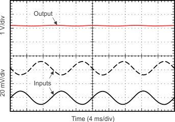
An example output response of a difference configuration is shown in Figure 8-6. The reference pin of the first channel is connected to a reference voltage of 2.048 V. The inputs to each circuit is a 100-Hz sine wave, 180° out-of-phase with each other, resulting in a zero output as shown. The sine wave input to the first circuit is offset so that the input wave is completely above GND.

| VREF = 2.048 V | ||