SLYS023A December 2020 – May 2022 INA229
PRODUCTION DATA
- 1 Features
- 2 Applications
- 3 Description
- 4 Revision History
- 5 Pin Configuration and Functions
- 6 Specifications
-
7 Detailed Description
- 7.1 Overview
- 7.2 Functional Block Diagram
- 7.3 Feature Description
- 7.4 Device Functional Modes
- 7.5 Programming
- 7.6 Register Maps
- 8 Application and Implementation
- 9 Power Supply Recommendations
- 10Layout
- 11Device and Documentation Support
- 12Mechanical, Packaging, and Orderable Information
Package Options
Mechanical Data (Package|Pins)
- DGS|10
Thermal pad, mechanical data (Package|Pins)
Orderable Information
7.3.5 Shunt Resistor Drift Compensation
The INA229 device has an internal temperature sensor which can measure die temperature from –40 °C to +125 °C. The accuracy of the temperature sensor is ±2 °C across the operational temperature range. The temperature value is stored inside the DIETEMP register and can be read through the digital interface.
The device has the capability to utilize the temperature measurement to compensate for shunt resistor temperature variance. This feature can be enabled by setting the TEMPCOMP bit in the CONFIG register, while the SHUNT_TEMPCO is the register that can be programmed to enter the temperature coefficient of the used shunt. The full scale value of the SHUNT_TEMPCO register is 16384 ppm/°C. The temperature compensation is referenced to +25 °C . The shunt is always assumed to have a positive temperature coefficient and the temperature compensation follows Equation 1:
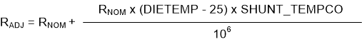
where
- RNOM is the nominal shunt resistance in Ohms at 25 °C.
- DIETEMP is the temperature value in the DIETEMP register in °C.
- SHUNT_TEMPCO is the shunt temperature coefficient in ppm/°C.
When this feature is enabled and correctly programmed, the CURRENT register data is corrected by constantly monitoring the die temperature and becomes a function of temperature. The effectiveness of the compensation will depend on how well the resistor and the INA229 are thermally coupled since the die temperature of the INA229 is used for the compensation.
Warning: If temperature compensation is enabled under some conditions, the calculated current result may be lower than the actual value. This condition typically occurs when there is a high value of shunt voltage ( >70% of full range), there is a shunt with high temperature-coefficient value ( >2000 ppm/°C), and there is a high temperature ( >100°C). Consider the example of constant current flowing through a high temperature coefficient shunt such that at lower temperatures the shunt voltage is in its upper range. As the temperature increases, the device will correctly report a constant current until the maximum shunt voltage is reached. As temperature continues to increase after the maximum shunt voltage is reached, the device will start reporting lower currents. This is because the effective resistance calculated will continue to increase while the detected shunt voltage will remain constant due to the voltage exceeding the selected ADC range.