SBOS844C May   2021  – March 2023 INA234

PRODUCTION DATA  

  1. Features
  2. Applications
  3. Description
  4. Revision History
  5. Pin Configuration and Functions
  6. Specifications
    1. 6.1 Absolute Maximum Ratings
    2. 6.2 ESD Ratings
    3. 6.3 Recommended Operating Conditions
    4. 6.4 Thermal Information
    5. 6.5 Electrical Characteristics
    6. 6.6 Timing Requirements (I2C)
    7. 6.7 Timing Diagram
    8. 6.8 Typical Characteristics
  7. Detailed Description
    1. 7.1 Overview
    2. 7.2 Functional Block Diagram
    3. 7.3 Feature Description
      1. 7.3.1 Integrated Analog-to-Digital Convertor (ADC)
      2. 7.3.2 Power Calculation
      3. 7.3.3 Low Bias Current
      4. 7.3.4 Low Voltage Supply and Wide Common-Mode Voltage Range
      5. 7.3.5 ALERT Pin
    4. 7.4 Device Functional Modes
      1. 7.4.1 Continuous Verses Triggered Operation
      2. 7.4.2 Device Shutdown
      3. 7.4.3 Power-On Reset
      4. 7.4.4 Averaging and Conversion Time Considerations
    5. 7.5 Programming
      1. 7.5.1 I2C Serial Interface
      2. 7.5.2 Writing to and Reading Through the I2C Serial Interface
      3. 7.5.3 High-Speed I2C Mode
      4. 7.5.4 General Call Reset
      5. 7.5.5 General Call Start Byte
      6. 7.5.6 SMBus Alert Response
    6. 7.6 Register Maps
      1. 7.6.1 Device Registers
  8. Application and Implementation
    1. 8.1 Application Information
      1. 8.1.1 Device Measurement Range and Resolution
      2. 8.1.2 Current and Power Calculations
      3. 8.1.3 ADC Output Data Rate and Noise Performance
      4. 8.1.4 Filtering and Input Considerations
    2. 8.2 Typical Application
      1. 8.2.1 Design Requirements
      2. 8.2.2 Detailed Design Procedure
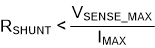
        1. 8.2.2.1 Select the Shunt Resistor
        2. 8.2.2.2 Configure the Device
        3. 8.2.2.3 Program the Shunt Calibration Register
        4. 8.2.2.4 Set Desired Fault Thresholds
        5. 8.2.2.5 Calculate Returned Values
      3. 8.2.3 Application Curves
    3. 8.3 Power Supply Recommendations
    4. 8.4 Layout
      1. 8.4.1 Layout Guidelines
      2. 8.4.2 Layout Example
  9. Device and Documentation Support
    1. 9.1 Device Support
      1. 9.1.1 Development Support
    2. 9.2 Documentation Support
      1. 9.2.1 Related Documentation
    3. 9.3 Receiving Notification of Documentation Updates
    4. 9.4 Support Resources
    5. 9.5 Trademarks
    6. 9.6 Electrostatic Discharge Caution
    7. 9.7 Glossary
  10. 10Mechanical, Packaging, and Orderable Information

Package Options

Refer to the PDF data sheet for device specific package drawings

Mechanical Data (Package|Pins)
  • YBJ|8
Thermal pad, mechanical data (Package|Pins)
Orderable Information

Select the Shunt Resistor

Using values from Table 8-3, the maximum value of the shunt resistor is calculated based on the value of the maximum current to be sensed (IMAX) and the maximum allowable sense voltage (VSENSE_MAX) for the chosen ADC range. When operating at the maximum current, the differential input voltage must not exceed the maximum full scale range of the device, VSENSE_MAX. Using Equation 5 for the given design parameters, the maximum value for RSHUNT is calculated to be 8.192 mΩ. The closest standard resistor value that is smaller than the maximum calculated value is 8.0 mΩ. Smaller resistors can be used to minimize power loss at the expense of reduced accuracy. The shunt resistor selected must have sufficient wattage to handle the power dissipation at maximum load at the desired operating temperature.

Equation 5. GUID-855C15C1-36C5-475A-A104-77BAB599B6D5-low.gif