SBOS445C July 2008 – December 2015 INA333
PRODUCTION DATA.
- 1 Features
- 2 Applications
- 3 Description
- 4 Revision History
- 5 Pin Configuration and Functions
- 6 Specifications
- 7 Detailed Description
- 8 Application and Implementation
- 9 Power Supply Recommendations
- 10Layout
- 11Device and Documentation Support
- 12Mechanical, Packaging, and Orderable Information
Package Options
Mechanical Data (Package|Pins)
Thermal pad, mechanical data (Package|Pins)
- DRG|8
Orderable Information
11 Device and Documentation Support
11.1 Device Support
11.1.1 Development Support
11.1.1.1 TINA-TI (Free Download Software)
Using TINA-TI SPICE-Based Analog Simulation Program with the INA333
TINA is a simple, powerful, and easy-to-use circuit simulation program based on a SPICE engine. TINA-TI is a free, fully functional version of the TINA software, preloaded with a library of macromodels in addition to a range of both passive and active models. It provides all the conventional DC, transient, and frequency domain analysis of SPICE as well as additional design capabilities.
Available as a free download from the Analog eLab Design Center, TINA-TI offers extensive post-processing capability that allows users to format results in a variety of ways.
Virtual instruments offer users the ability to select input waveforms and probe circuit nodes, voltages, and waveforms, creating a dynamic quick-start tool.
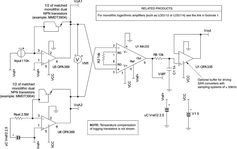
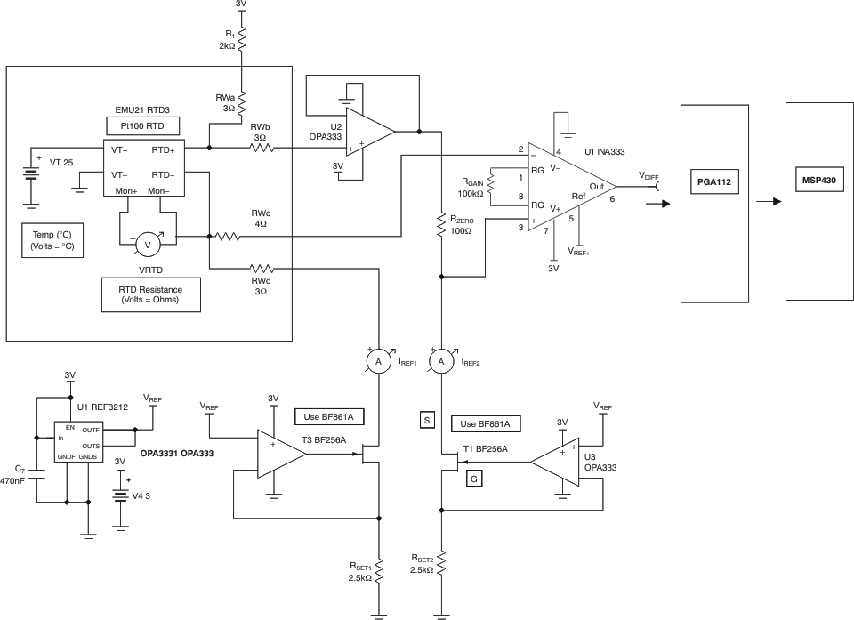
Figure 41 and Figure 42 show example TINA-TI circuits for the INA333 device that can be used to develop, modify, and assess the circuit design for specific applications. Links to download these simulation files are given below.
NOTE
These files require that either the TINA software (from DesignSoft) or TINA-TI software be installed. Download the free TINA-TI software from the TINA-TI folder.

NOINDENT:
The following link launches the TI logarithmic amplifiers web page: Logarithmic Amplifier Products Home Page(Example Glucose Meter)
To download a compressed file that contains the TINA-TI simulation file for this circuit, click the following link: Log Circuit.

NOINDENT:
RWa, RWb, RWc, and RWd simulate wire resistance. These resistors are included to show the four-wire sense technique immunity to line mismatches. This method assumes the use of a four-wire RTD.To download a compressed file that contains the TINA-TI simulation file for this circuit, click the following link: PT100 RTD.
11.2 Documentation Support
11.2.1 Related Documentation
For related documentation see the following:
11.3 Trademarks
All trademarks are the property of their respective owners.
11.4 Electrostatic Discharge Caution

These devices have limited built-in ESD protection. The leads should be shorted together or the device placed in conductive foam during storage or handling to prevent electrostatic damage to the MOS gates.
11.5 Glossary
SLYZ022 — TI Glossary.
This glossary lists and explains terms, acronyms, and definitions.