SBOS445C July   2008  – December 2015 INA333

PRODUCTION DATA.  

  1. Features
  2. Applications
  3. Description
  4. Revision History
  5. Pin Configuration and Functions
  6. Specifications
    1. 6.1 Absolute Maximum Ratings
    2. 6.2 ESD Ratings
    3. 6.3 Recommended Operating Conditions
    4. 6.4 Thermal Information
    5. 6.5 Electrical Characteristics
    6. 6.6 Typical Characteristics
  7. Detailed Description
    1. 7.1 Overview
    2. 7.2 Functional Block Diagram
    3. 7.3 Feature Description
    4. 7.4 Device Functional Modes
      1. 7.4.1 Internal Offset Correction
      2. 7.4.2 Input Common-Mode Range
  8. Application and Implementation
    1. 8.1 Application Information
    2. 8.2 Typical Application
      1. 8.2.1 Design Requirements
      2. 8.2.2 Detailed Design Procedure
        1. 8.2.2.1  Setting the Gain
        2. 8.2.2.2  Internal Offset Correction
        3. 8.2.2.3  Offset Trimming
        4. 8.2.2.4  Noise Performance
        5. 8.2.2.5  Input Bias Current Return Path
        6. 8.2.2.6  Input Common-Mode Range
        7. 8.2.2.7  Operating Voltage
        8. 8.2.2.8  Low Voltage Operation
        9. 8.2.2.9  Single-Supply Operation
        10. 8.2.2.10 Input Protection
      3. 8.2.3 Application Curves
  9. Power Supply Recommendations
  10. 10Layout
    1. 10.1 Layout Guidelines
    2. 10.2 Layout Example
  11. 11Device and Documentation Support
    1. 11.1 Device Support
      1. 11.1.1 Development Support
        1. 11.1.1.1 TINA-TI (Free Download Software)
    2. 11.2 Documentation Support
      1. 11.2.1 Related Documentation
    3. 11.3 Trademarks
    4. 11.4 Electrostatic Discharge Caution
    5. 11.5 Glossary
  12. 12Mechanical, Packaging, and Orderable Information

Package Options

Mechanical Data (Package|Pins)
Thermal pad, mechanical data (Package|Pins)
Orderable Information

5 Pin Configuration and Functions

DGK Package
8-Pin VSSOP
Top View
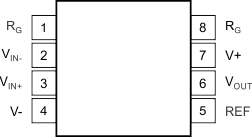
INA333 po_msop_bos445.gif
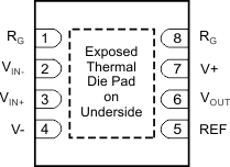
DRG Package
8-Pin WSON
Top View
INA333 po_dfn_bos445.gif

Pin Functions

PIN I/O DESCRIPTION
NAME NO.
REF 5 I Reference input. This pin must be driven by low impedance or connected to ground.
RG 1, 8 Gain setting pins. For gains greater than 1, place a gain resistor between pins 1 and 8.
V+ 7 Positive supply
V 4 Negative supply
VIN+ 3 I Positive input
VIN– 2 I Negative input
VOUT 6 O Output