SBOS914F October 2018 – April 2021 INA592
PRODUCTION DATA
- 1 Features
- 2 Applications
- 3 Description
- 4 Revision History
- 5 Device Comparison Table
- 6 Pin Configuration and Functions
- 7 Specifications
- 8 Detailed Description
- 9 Application and Implementation
- 10Power Supply Recommendations
- 11Layout
- 12Device and Documentation Support
- 13Mechanical, Packaging, and Orderable Information
Package Options
Mechanical Data (Package|Pins)
Thermal pad, mechanical data (Package|Pins)
- DRC|10
Orderable Information
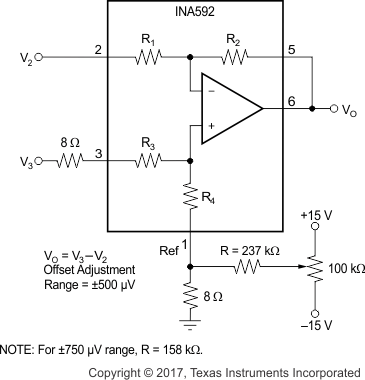
9.2.1.2.2 Offset Voltage Trim
The INA592 is production trimmed for low offset voltage and drift. Most applications require no external offset adjustment. Figure 9-2 shows an optional circuit for trimming the output offset voltage. The output is referred to the output reference terminal (pin 1), which is normally grounded. A voltage applied to the REF pin is summed with the output signal. This summing operation can be used to null offset voltage. To maintain good common-mode rejection, the source impedance of a signal applied to the REF pin must be less than 8 Ω. For low impedance at the REF pin, the trim voltage can be buffered with an op amp, such as the OPA177.
 Figure 9-2 Offset Adjustment