SBOS385B August 2019 – April 2021 INA597
PRODUCTION DATA
- 1 Features
- 2 Applications
- 3 Description
- 4 Revision History
- 5 Device Comparison Table
- 6 Pin Configuration and Functions
- 7 Specifications
- 8 Detailed Description
-
9 Application and Implementation
- 9.1 Application Information
- 9.2
Typical Applications
- 9.2.1 Basic Power-Supply and Signal Connections
- 9.2.2 Precision Instrumentation Amplifier
- 9.2.3 Low Power, High-Output Current, Precision, Difference Amplifier
- 9.2.4 Pseudoground Generator
- 9.2.5 Differential Input Data Acquisition
- 9.2.6 Precision Voltage-to-Current Conversion
- 9.2.7 Additional Applications
- 10Power Supply Recommendations
- 11Layout
- 12Device and Documentation Support
- 13Mechanical, Packaging, and Orderable Information
Package Options
Mechanical Data (Package|Pins)
Thermal pad, mechanical data (Package|Pins)
- DRC|10
Orderable Information
3 Description
The INA597 is a low-power, wide-bandwidth, difference amplifier for cost-sensitive applications. The INA597 consists of a precision operational amplifier (op amp) and a precision resistor network. Excellent tracking of resistors maintains gain accuracy and common-mode rejection over temperature. Unique features such as low offset (200 μV, maximum), low offset drift (5 μV/°C maximum) high slew rate (18 V/μs), and high capacitive load drive of up to 500 pF make the INA597 a robust, high-performance difference amplifier for high-voltage industrial applications.
The common-mode range of the internal op amp extends to the negative supply, and enables the device to operate in single-supply applications. The device operates on single (4.5 V to 36 V) or dual supplies (±2.25 V to ±18 V).
The difference amplifier is the foundation of many commonly used circuits. The INA597 provides this circuit function without using an expensive precision resistor network.
| PART NUMBER | PACKAGE(1) | BODY SIZE (NOM) |
|---|---|---|
| INA597 | SOIC (8) | 4.90 mm × 3.91 mm |
| VSON (10) | 3.00 mm × 3.00 mm | |
| VSSOP (8) | 3.00 mm × 3.00 mm |
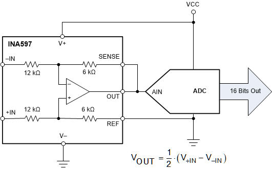
 Differential Input Data
Acquisition
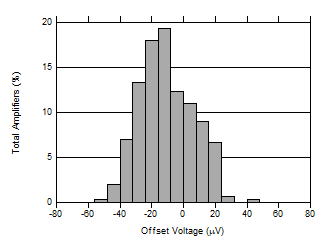
 Typical Distribution of
Offset Voltage (RTO)
 G = 1/2, VS = ±18 V