SBOS385B August 2019 – April 2021 INA597
PRODUCTION DATA
- 1 Features
- 2 Applications
- 3 Description
- 4 Revision History
- 5 Device Comparison Table
- 6 Pin Configuration and Functions
- 7 Specifications
- 8 Detailed Description
-
9 Application and Implementation
- 9.1 Application Information
- 9.2
Typical Applications
- 9.2.1 Basic Power-Supply and Signal Connections
- 9.2.2 Precision Instrumentation Amplifier
- 9.2.3 Low Power, High-Output Current, Precision, Difference Amplifier
- 9.2.4 Pseudoground Generator
- 9.2.5 Differential Input Data Acquisition
- 9.2.6 Precision Voltage-to-Current Conversion
- 9.2.7 Additional Applications
- 10Power Supply Recommendations
- 11Layout
- 12Device and Documentation Support
- 13Mechanical, Packaging, and Orderable Information
Package Options
Mechanical Data (Package|Pins)
Thermal pad, mechanical data (Package|Pins)
- DRC|10
Orderable Information
9.2.1.2.3 Input Voltage Range
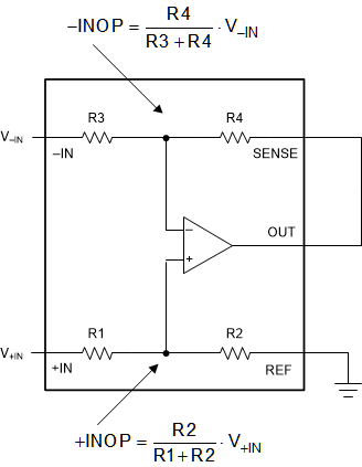
The INA597 measures input voltages beyond the supply rails. The internal resistors divide down the voltage before the voltage reaches the internal op amp and provide protection to the op amp inputs. Figure 9-3 shows an example of how the voltage division works in a difference-amplifier configuration. For the INA597 to measure correctly, the input voltages at the input nodes of the internal op amp must stay less than 0.1 V of the positive supply rail, and can exceed the negative supply rail by 0.1 V. See Section 10 for more details.
 Figure 9-3 Voltage Division in the Difference Amplifier Configuration
The INA597 has integrated ESD diodes at the inputs that provide overvoltage protection. This feature simplifies system design by eliminating the need for additional external protection circuitry, and enables a more robust system. The voltages at any of the inputs of the parts in G = ½ configuration with ±18 V supplies can safely range from +VS − 54 V up to −VS + 54 V. For example, on ±10-V supplies, the input voltages can go as high as ±30 V.