SBOS631B June 2012 – November 2017 INA827
PRODUCTION DATA.
- 1 Features
- 2 Applications
- 3 Description
- 4 Revision History
- 5 Pin Configuration and Functions
- 6 Specifications
- 7 Typical Characteristics
- 8 Detailed Description
- 9 Application and Implementation
- 10Power Supply Recommendations
- 11Layout
- 12Device and Documentation Support
- 13Mechanical, Packaging, and Orderable Information
Package Options
Mechanical Data (Package|Pins)
- DGK|8
Thermal pad, mechanical data (Package|Pins)
Orderable Information
9 Application and Implementation
NOTE
Information in the following applications sections is not part of the TI component specification, and TI does not warrant its accuracy or completeness. TI’s customers are responsible for determining suitability of components for their purposes. Customers should validate and test their design implementation to confirm system functionality.
9.1 Application Information
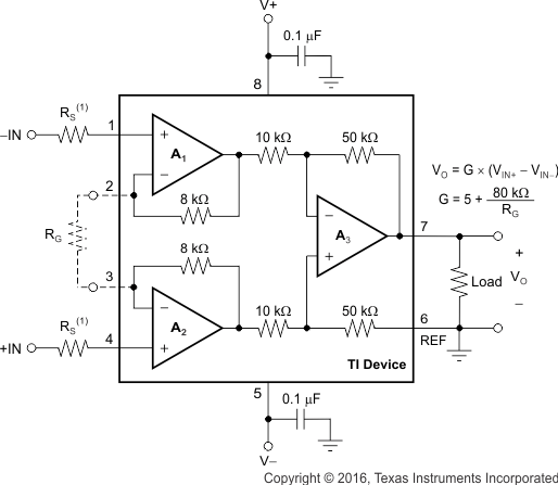
Figure 61 shows the basic connections required for device operation. Good layout practice mandates that bypass capacitors are placed as close to the device pins as possible.
The INA827 output is referred to the output reference (REF) pin, which is normally grounded. This connection must be low-impedance to assure good common-mode rejection. Although 5 Ω or less of stray resistance can be tolerated when maintaining specified CMRR, small stray resistances of tens of ohms in series with the REF pin can cause noticeable degradation in CMRR.

NOINDENT:
This resistor is optional if the input voltage remains above [(V–) – 2 V] or if the signal source current drive capability is limited to less than 3.5 mA. See the Input Protection section for more details.9.2 Typical Application
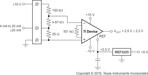
An example programmable logic controller (PLC) input application using an INA827 is shown in Figure 62.
 Figure 62. ±10-V, 4-mA to 20-mA PLC Input
9.2.1 Design Requirements
This design has these requirements:
- Supply voltage: ±15 V, 5 V
- Inputs: ±10 V, ±20 mA
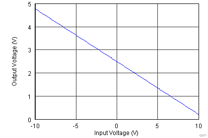
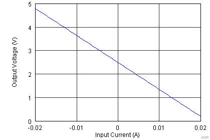
- Output: 2.5 V, ±2.3 V
9.2.2 Detailed Design Procedure
There are two modes of operation for the circuit shown in Figure 62: current input and voltage input. This design requires R1 >> R2 >> R3. Given this relationship, the current input mode transfer function is given by Equation 2.

where
- G represents the gain of the instrumentation amplifier
The transfer function for the voltage input mode is shown by Equation 3.

R1 sets the input impedance of the voltage input mode. The minimum typical input impedance is 100 kΩ. 100 kΩ is selected for R1 because increasing the R1 value also increases noise. The value of R3 must be extremely small compared to R1 and R2. 20 Ω for R3 is selected because that resistance value is much smaller than R1 and yields an input voltage of ±400 mV when operated in current mode (±20 mA).
Equation 4 can be used to calculate R2 given VD = ±400 mV, VIN = ±10 V, and R1 = 100 kΩ.

The value obtained from Equation 4 is not a standard 0.1% value, so 4.12 kΩ is selected. R1 and R2 also use 0.1% tolerance resistors to minimize error.
The ideal gain of the instrumentation amplifier is calculated with Equation 5.

Using the INA827 gain equation, the gain-setting resistor value is calculated as shown by Equation 6.

107 kΩ is a standard 0.1% resistor value that can be used in this design. Finally, the output RC filter components are selected to have a –3-dB cutoff frequency of 1 MHz.
9.2.3 Application Curves

