SBOS631B June   2012  – November 2017 INA827

PRODUCTION DATA.  

  1. Features
  2. Applications
  3. Description
  4. Revision History
  5. Pin Configuration and Functions
  6. Specifications
    1. 6.1 Absolute Maximum Ratings
    2. 6.2 ESD Ratings
    3. 6.3 Recommended Operating Conditions
    4. 6.4 Thermal Information
    5. 6.5 Electrical Characteristics
  7. Typical Characteristics
  8. Detailed Description
    1. 8.1 Overview
    2. 8.2 Functional Block Diagram
    3. 8.3 Feature Description
      1. 8.3.1  Setting the Gain
        1. 8.3.1.1 Gain Drift
      2. 8.3.2  Offset Trimming
      3. 8.3.3  Input Common-Mode Range
      4. 8.3.4  Inside the INA827
      5. 8.3.5  Input Protection
      6. 8.3.6  Input Bias Current Return Path
      7. 8.3.7  Reference Pin
      8. 8.3.8  Dynamic Performance
      9. 8.3.9  Operating Voltage
        1. 8.3.9.1 Low-Voltage Operation
      10. 8.3.10 Error Sources
    4. 8.4 Device Functional Modes
  9. Application and Implementation
    1. 9.1 Application Information
    2. 9.2 Typical Application
      1. 9.2.1 Design Requirements
      2. 9.2.2 Detailed Design Procedure
      3. 9.2.3 Application Curves
  10. 10Power Supply Recommendations
  11. 11Layout
    1. 11.1 Layout Guidelines
      1. 11.1.1 CMRR vs Frequency
    2. 11.2 Layout Example
  12. 12Device and Documentation Support
    1. 12.1 Documentation Support
      1. 12.1.1 Related Documentation
    2. 12.2 Receiving Notification of Documentation Updates
    3. 12.3 Community Resources
    4. 12.4 Trademarks
    5. 12.5 Electrostatic Discharge Caution
    6. 12.6 Glossary
  13. 13Mechanical, Packaging, and Orderable Information

Package Options

Mechanical Data (Package|Pins)
Thermal pad, mechanical data (Package|Pins)
Orderable Information

Typical Characteristics

at TA = +25°C, VS = ±15 V, RL = 10 kΩ, VREF = 0 V, and G = 5 (unless otherwise noted)
INA827 tc_1_vosi_distri_bos631.png
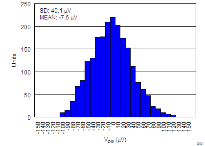
Figure 1. Typical Distribution of Input Offset Voltage
INA827 tc_2_voso_distri_bos631.png
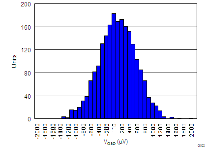
Figure 3. Typical Distribution of Output Offset Voltage
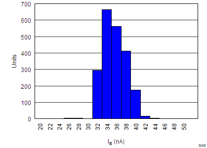
INA827 tc_5_ib_distri_bos631.png
Figure 5. Typical Distribution of Input Bias Current
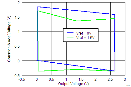
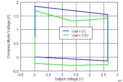
INA827 tc_7_common_mode_vs_output_1_bos631 rev1.png
Single supply, VS = +3 V, G = 5
Figure 7. Input Common-Mode Voltage vs Output Voltage
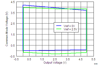
INA827 tc_9_common_mode_vs_output_3_bos631.png
Single supply, VS = +5 V, G = 5
Figure 9. Input Common-Mode Voltage vs Output Voltage
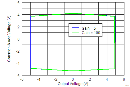
INA827 tc_11_common_mode_vs_output_5_bos631.png
Dual supply, VS = ±5 V
Figure 11. Input Common-Mode Voltage vs Output Voltage
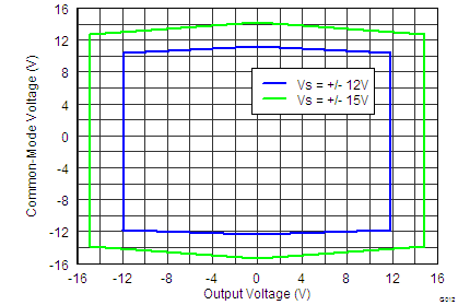
INA827 tc_13_common_mode_vs_output_7_bos631.png
Dual supply, VS = ±15 V, ±12 V, G = 100
Figure 13. Input Common-Mode Voltage vs Output Voltage
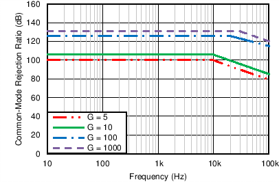
INA827 C015_SBOS631.png
Figure 15. CMRR vs Frequency (RTI)
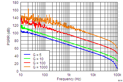
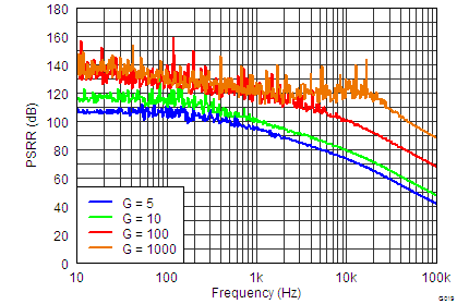
INA827 tc_18_psrr_pos_bos631.png
Figure 17. Positive PSRR vs Frequency (RTI)
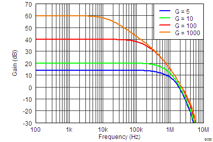
INA827 tc_22_gain_vs_frequency_bos631.png
Figure 19. Gain vs Frequency
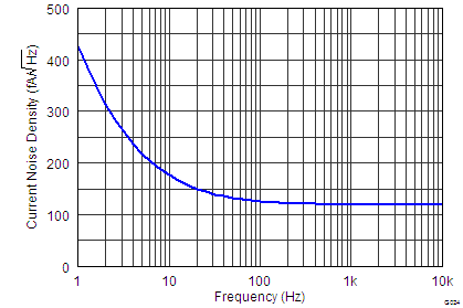
INA827 tc_24_current_noise_density_bos631.png
Figure 21. Current Noise Spectral Density vs Frequency (RTI)
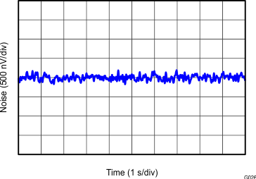
INA827 tc_26_low_freq_voltage_noise_2_bos631.gif
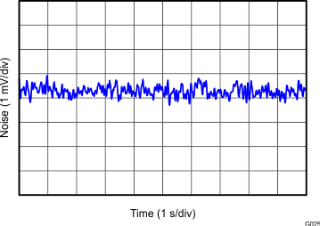
Figure 23. 0.1-Hz to 10-Hz RTI Voltage Noise (G = 1000)
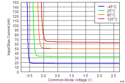
INA827 tc_28_bias_current_vs_common_mode_1_bos631.png
VS = +2.7 V
Figure 25. Input Bias Current vs Common-Mode Voltage
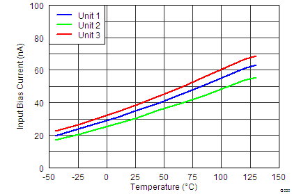
INA827 tc_30_bias_current_vs_temperature_bos631.png
Figure 27. Input Bias Current vs Temperature
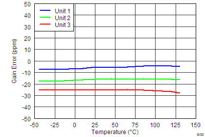
INA827 tc_32_gain_vs_temperature_bos631.png
Figure 29. Gain Error vs Temperature (G = 5)
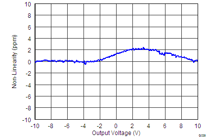
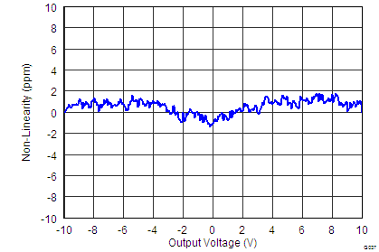
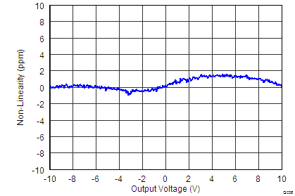
INA827 tc_35_gain_nonlinearity_1_bos631.png
Figure 31. Gain Nonlinearity (G = 5)
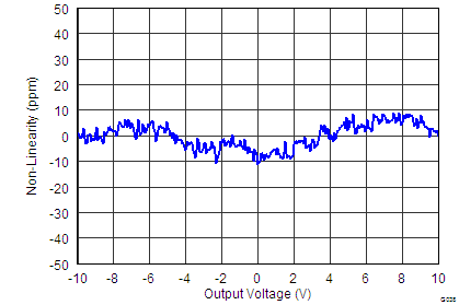
INA827 tc_37_gain_nonlinearity_3_bos631.png
Figure 33. Gain Nonlinearity (G = 100)
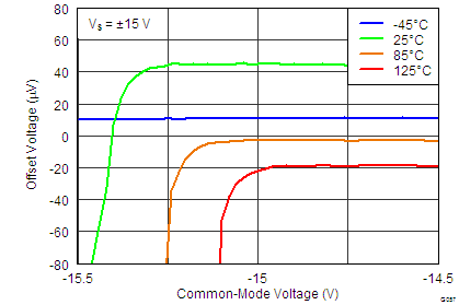
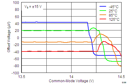
INA827 tc_57_v_os_vs_v_cm_1_bos631.png
VS = ±15 V
Figure 35. Offset Voltage vs
Negative Common-Mode Voltage
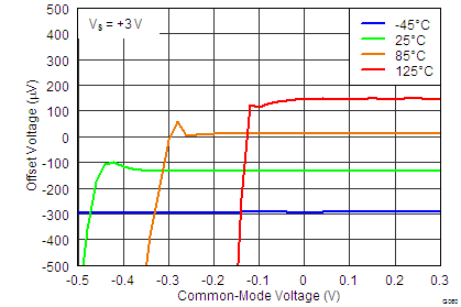
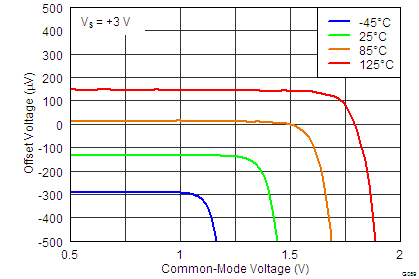
INA827 tc_59_v_os_vs_v_cm_3_bos631 rev 1.png
VS = +3 V
Figure 37. Offset Voltage vs
Negative Common-Mode Voltage
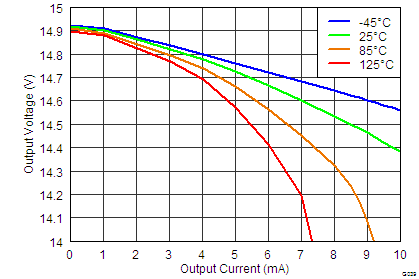
INA827 tc_39_pos_output_swing_bos631.png
VS = ±15 V
Figure 39. Positive Output Voltage Swing vs
Output Current
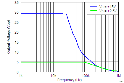
INA827 tc_43_large_signal_bos631.png
Figure 41. Large-Signal Frequency Response
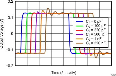
INA827 tc_45_capacitive_load_bos631.gif
Figure 43. Small-Signal Response Over Capacitive Loads
(G = 5)
INA827 tc_52_small_signal_response_2_bos631.gif
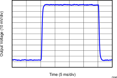
G = 10, RL = 10 kΩ, CL = 100 pF
Figure 45. Small-Signal Response
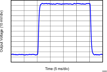
INA827 tc_54_small_signal_response_4_bos631.gif
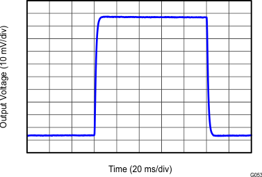
G = 1000, RL = 10 kΩ, CL = 100 pF
Figure 47. Small-Signal Response
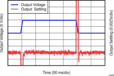
INA827 tc_62_large_signal_3_bos631.gif
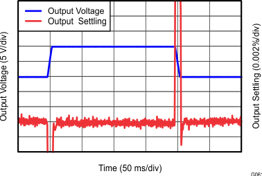
G = 10, RL = 10 kΩ, CL = 100 pF
Figure 49. Large-Signal Response and Settling Time
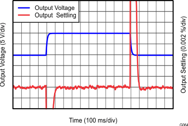
INA827 tc_64_large_signal_5_bos631.gif
G = 1000, RL = 10 kΩ, CL = 100 pF
Figure 51. Large-Signal Response and Settling Time
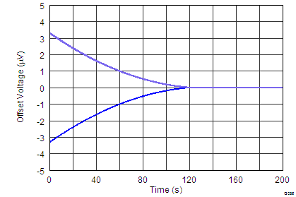
INA827 tc_56_warm_up_bos631.png
Figure 53. Change In Input Offset Voltage vs Warm-Up Time
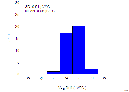
INA827 tc_2_vosi_drift_distri_bos631.png
Figure 2. Typical Distribution of Input Offset Voltage Drift
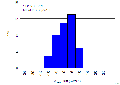
INA827 tc_4_voso_drift_distri_bos631.png
Figure 4. Typical Distribution of Output Offset Voltage Drift
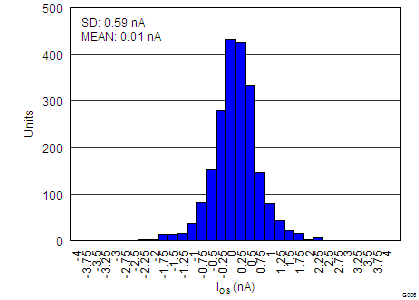
INA827 tc_6_ios_distri_bos631.png
Figure 6. Typical Distribution of Input Offset Current
INA827 tc_8_common_mode_vs_output_2_bos631 rev1.png
Single supply, VS = +3 V, G = 100
Figure 8. Input Common-Mode Voltage vs Output Voltage
INA827 tc_10_common_mode_vs_output_4_bos631.png
Single supply, VS = +5 V, G = 100
Figure 10. Input Common-Mode Voltage vs Output Voltage
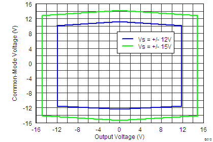
INA827 tc_12_common_mode_vs_output_6_bos631.png
Dual supply, VS = ±15 V, ±12 V, G = 5
Figure 12. Input Common-Mode Voltage vs Output Voltage
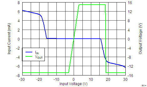
INA827 tc_14_overvoltage_vs_current_1_bos631.png
G = 1, VS = ±15 V
Figure 14. Input Overvoltage vs Input Current
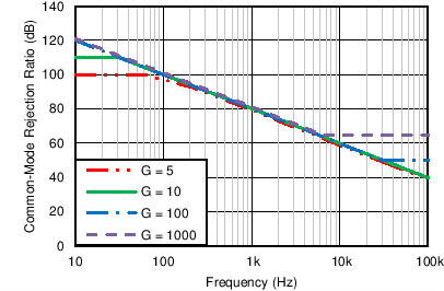
INA827 C016_SBOS631.png
1-kΩ source imbalance
Figure 16. CMRR vs Frequency (RTI)
INA827 tc_19_psrr_neg_bos631.png
Figure 18. Negative PSRR vs Frequency (RTI)
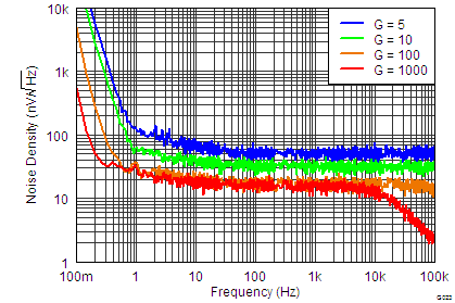
INA827 tc_23_voltage_noise_density_bos631.png
Figure 20. Voltage Noise Spectral Density vs Frequency (RTI)
INA827 tc_25_low_freq_voltage_noise_1_bos631.gif
Figure 22. 0.1-Hz to 10-Hz RTI Voltage Noise (G = 5)
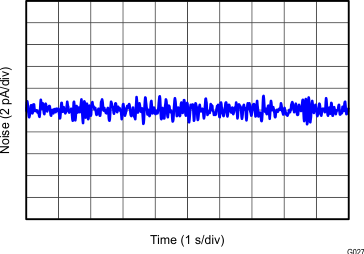
INA827 tc_27_low_freq_current_noise_bos631.gif
Figure 24. 0.1-Hz to 10-Hz RTI Current Noise
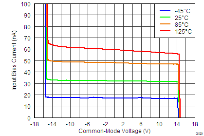
INA827 tc_29_bias_current_vs_common_mode_2_bos631.png
VS = ±15 V
Figure 26. Input Bias Current vs Common-Mode Voltage
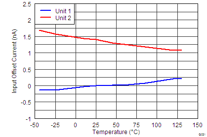
INA827 tc_31_offset_current_vs_temperature_bos631.png
Figure 28. Input Offset Current vs Temperature
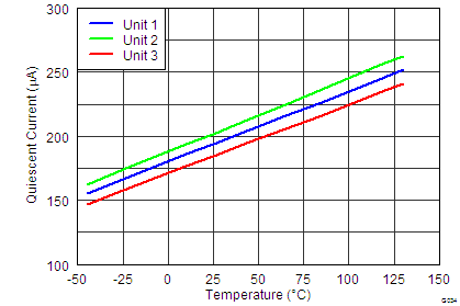
INA827 tc_34_supply_current_vs_temperature_bos631.png
Figure 30. Supply Current vs Temperature
INA827 tc_36_gain_nonlinearity_2_bos631.png
Figure 32. Gain Nonlinearity (G = 10)
INA827 tc_38_gain_nonlinearity_4_bos631.png
Figure 34. Gain Nonlinearity (G = 1000)
INA827 tc_58_v_os_vs_v_cm_2_bos631.png
VS = ±15 V
Figure 36. Offset Voltage vs
Positive Common-Mode Voltage
INA827 tc_60_v_os_vs_v_cm_4_bos631 rev1.png
VS = +3 V
Figure 38. Offset Voltage vs
Positive Common-Mode Voltage
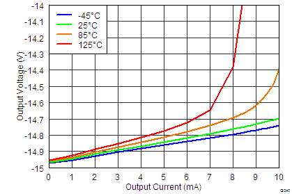
INA827 tc_40_neg_output_swing_bos631.png
VS = ±15 V
Figure 40. Negative Output Voltage Swing vs
Output Current
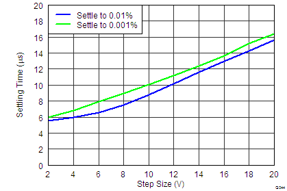
INA827 tc_44_settling_time_bos631.png
VS = ±15 V
Figure 42. Settling Time vs Step Size
INA827 tc_46_small_signal_response_1_bos631.gif
G = 5, RL = 1 kΩ, CL = 100 pF
Figure 44. Small-Signal Response
INA827 tc_53_small_signal_response_3_bos631.gif
G = 100, RL = 10 kΩ, CL = 100 pF
Figure 46. Small-Signal Response
INA827 tc_61_large_signal_2_bos631.gif
G = 5, RL = 10 kΩ, CL = 100 pF
Figure 48. Large-Signal Response and Settling Time
INA827 tc_63_large_signal_4_bos631.gif
G = 100, RL = 10 kΩ, CL = 100 pF
Figure 50. Large-Signal Response and Settling Time
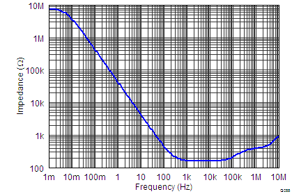
INA827 tc_55_open_loop_impedance_bos631.png
Figure 52. Open-Loop Output Impedance