SBOS792A August 2017 – January 2018 INA828
PRODUCTION DATA.
- 1 Features
- 2 Applications
- 3 Description
- 4 Revision History
- 5 Pin Configuration and Functions
- 6 Specifications
- 7 Detailed Description
- 8 Application and Implementation
- 9 Power Supply Recommendations
- 10Layout
- 11Device and Documentation Support
- 12Mechanical, Packaging, and Orderable Information
Package Options
Mechanical Data (Package|Pins)
- D|8
Thermal pad, mechanical data (Package|Pins)
Orderable Information
8.1 Reference Terminal
The output voltage of the INA828 is developed with respect to the voltage on the reference terminal, REF. Often, in dual-supply operation, the reference pin (pin 6) is connected to the low-impedance system ground. In single-supply operation, offsetting the output signal to a precise mid-supply level is useful (for example, 2.5 V in a 5-V supply environment). To accomplish this level shift, a voltage source must be connected to the REF pin to level-shift the output so that the INA828 can drive a single-supply ADC.
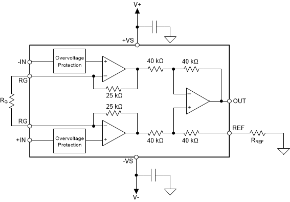
The voltage source applied to the reference terminal must have a low output impedance. As illustrated in Figure 61, any resistance at the reference terminal (shown as RREF in Figure 61) is in series with one of the internal 40-kΩ resistors.
 Figure 61. Parasitic Resistance Shown at the Reference Terminal
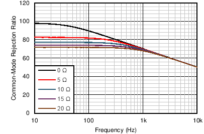
The parasitic resistance at the reference terminal, RREF, creates an imbalance in the 4 resistors of the internal difference amplifier, resulting in degraded common-mode rejection ratio (CMRR). Figure 62 shows the degradation in CMRR of the INA828 for increasing resistance at the reference terminal. For the best performance, keep the source impedance to the REF terminal, RREF, below 5 Ω.
 Figure 62. The Effect of Increasing Resistance at the Reference Terminal
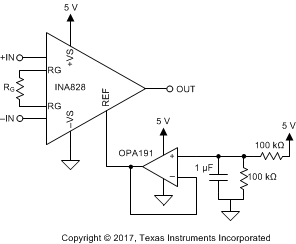
Voltage reference ICs are an excellent option for providing a low-impedance voltage source for the reference terminal. However, if a resistor voltage divider is used to generate a reference voltage, it must be buffered by an op amp as shown in Figure 63 to avoid CMRR degradation.
 Figure 63. Using an Op Amp to Buffer Reference Voltages