SLLS983L June 2009 – October 2023 ISO1050
PRODUCTION DATA
- 1
- 1 Features
- 2 Applications
- 3 Description
- 4 Revision History
- 5 Pin Configuration and Functions
-
6 Specifications
- 6.1 Absolute Maximum Ratings
- 6.2 ESD Ratings
- 6.3 Recommended Operating Conditions
- 6.4 Thermal Information
- 6.5 Power Ratings
- 6.6 Insulation Specifications
- 6.7 Safety-Related Certifications
- 6.8 Safety Limiting Values
- 6.9 Electrical Characteristics - DC Specification
- 6.10 Switching Characteristics
- 6.11 Insulation Characteristics Curves
- 6.12 Typical Characteristics
- 7 Parameter Measurement Information
- 8 Detailed Description
- 9 Application and Implementation
- 10Power Supply Recommendations
- 11Layout
- 12Device and Documentation Support
- 13Mechanical, Packaging, and Orderable Information
Package Options
Mechanical Data (Package|Pins)
Thermal pad, mechanical data (Package|Pins)
- DUB|8
Orderable Information
6.12 Typical Characteristics
 Figure 6-3 Recessive-to-Dominant Loop Time vs Free-Air Temperature (Across Vcc)
 Figure 6-5 Supply Current
(RMS) vs Signaling Rate (kbps)
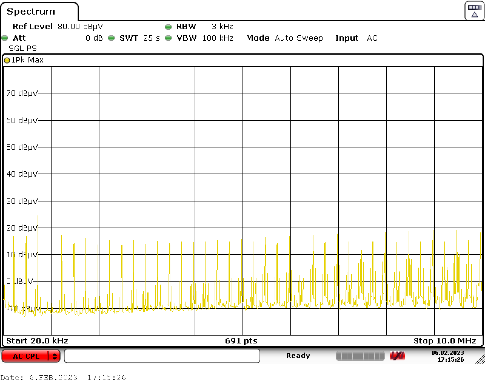
 Figure 6-7 Emissions
Spectrum to 10 MHz
 Figure 6-4 Dominant-to-Recessive Loop Time vs Free-Air Temperature (Across Vcc)
 Figure 6-6 Driver Output
Voltage vs Free-Air Temperature
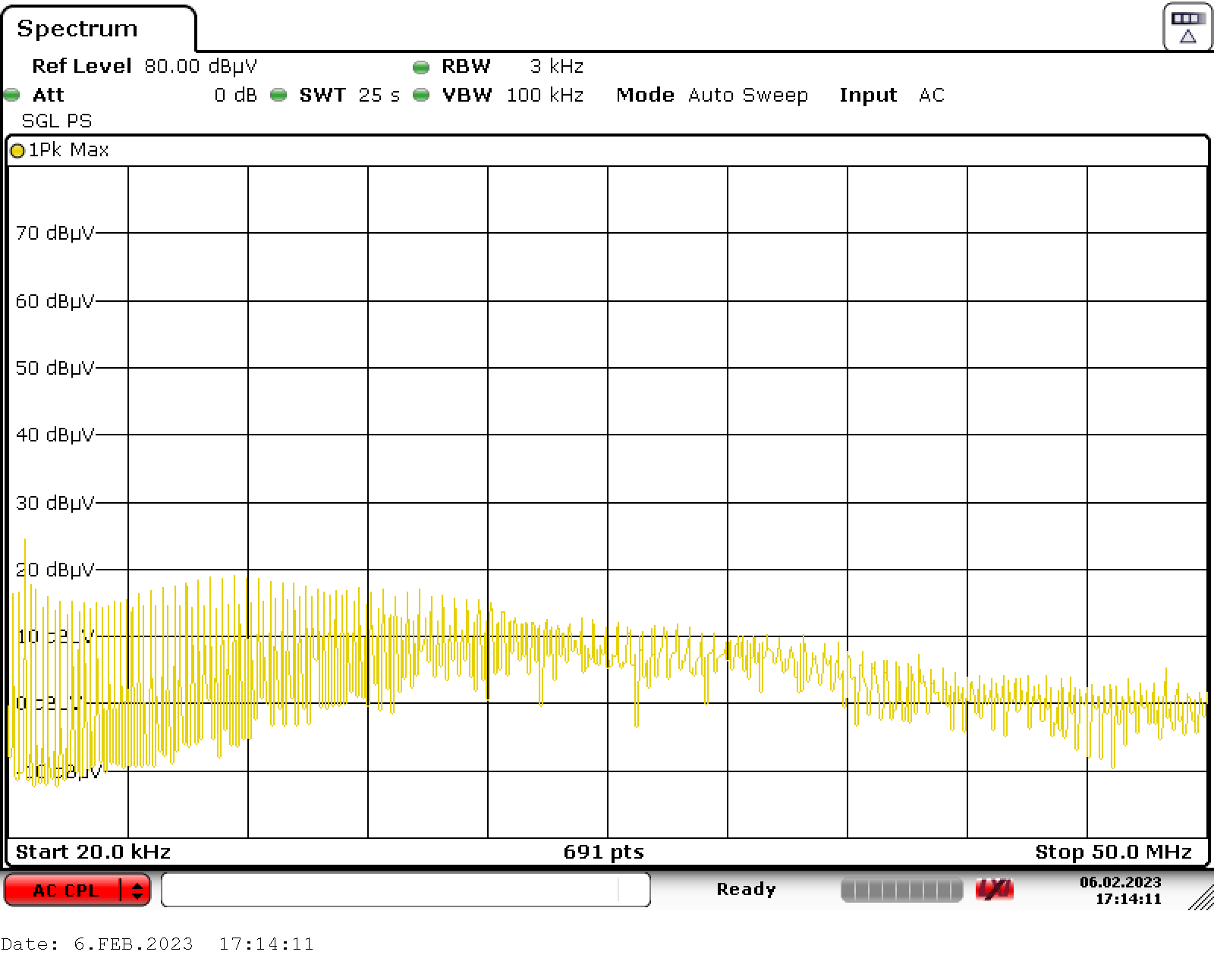
 Figure 6-8 Emissions
Spectrum to 50 MHz