SLLS983L June 2009 – October 2023 ISO1050
PRODUCTION DATA
- 1
- 1 Features
- 2 Applications
- 3 Description
- 4 Revision History
- 5 Pin Configuration and Functions
-
6 Specifications
- 6.1 Absolute Maximum Ratings
- 6.2 ESD Ratings
- 6.3 Recommended Operating Conditions
- 6.4 Thermal Information
- 6.5 Power Ratings
- 6.6 Insulation Specifications
- 6.7 Safety-Related Certifications
- 6.8 Safety Limiting Values
- 6.9 Electrical Characteristics - DC Specification
- 6.10 Switching Characteristics
- 6.11 Insulation Characteristics Curves
- 6.12 Typical Characteristics
- 7 Parameter Measurement Information
- 8 Detailed Description
- 9 Application and Implementation
- 10Power Supply Recommendations
- 11Layout
- 12Device and Documentation Support
- 13Mechanical, Packaging, and Orderable Information
Package Options
Mechanical Data (Package|Pins)
Thermal pad, mechanical data (Package|Pins)
Orderable Information
10.2 Power Supply Discharging
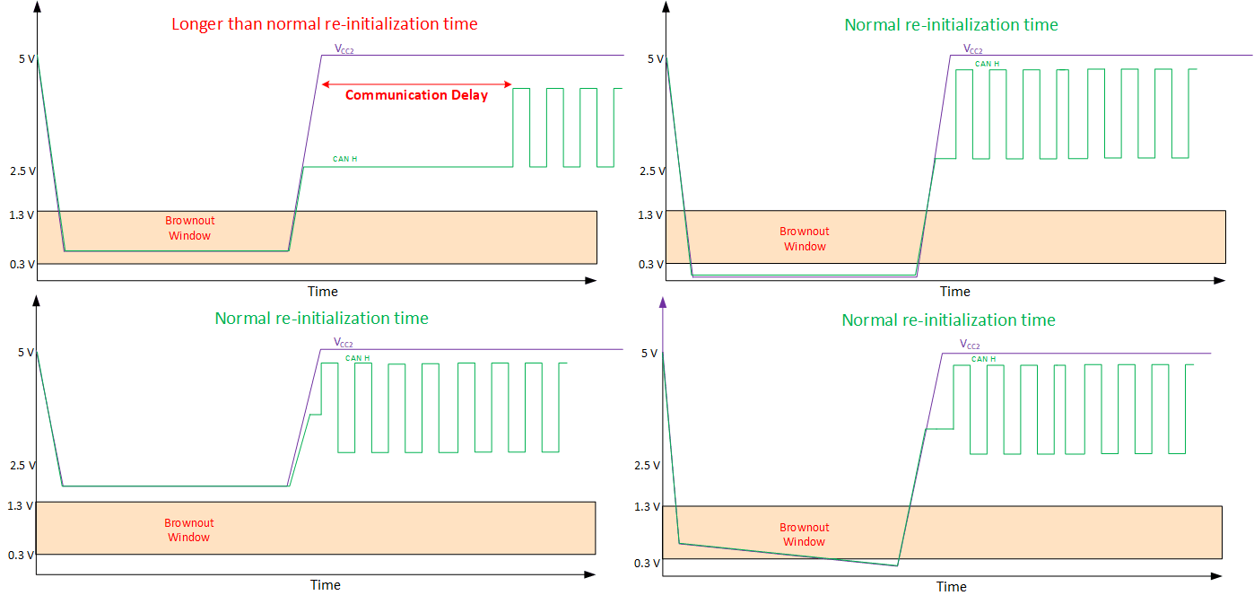
To ensure normal re-initialization time after a power down, the power supply for the ISO1050 needs to discharge below 0.3 V, and as closely to 0 V as possible, to ensure that a communication delay does not occur. Figure 10-1 illustrates various scenarios of power-supply ramp-down and its effect on the communication delay.
 Figure 10-1 Power Supply Ramp-Down and Communication Delay Behavior
The brownout window, 0.3 V to 1.3 V (typical), represents the range of voltage in which a longer than normal re-initialization time may occur if VCC2 powers up from this voltage. The ISO1042, an upgraded device with higher isolation rating, CAN FD speeds of 5 Mbps, higher bus fault-protection voltage, stronger EMC performance, and smaller package options does not exhibit this behavior. For all new isolated CAN designs, it is recommended to use the ISO1042. If the ISO1050 must be used, ensure that VCC2 discharges to 0 V so that a longer than normal re-initialization time does not exist. If the power supplies cannot be configured in such a way that VCC2 discharge below 0.3 V on their own, implement a bleed resistor between VCC2 and GND2. The bleed resistor value should be selected such that it ensures VCC2 goes below the brownout window fast enough for any power interruption or power down sequence the system may permit. The lower the resistance, the faster VCC2 will discharge to 0V with the tradeoff of consuming power. For many systems, a bleed resistor value of 2 KΩ is sufficient.