SBOS074E September 1997 – June 2018 ISO124
PRODUCTION DATA.
- 1 Features
- 2 Applications
- 3 Description
- 4 Revision History
- 5 Pin Configuration and Functions
- 6 Specifications
- 7 Detailed Description
-
8 Application and Implementation
- 8.1 Application Information
- 8.2
Typical Applications
- 8.2.1 Output Filters
- 8.2.2 Battery Monitor
- 8.2.3 Programmable Gain Amplifier
- 8.2.4 Thermocouple Amplifier
- 8.2.5 Isolated 4-mA to 20-mA Instrument Loop
- 8.2.6 Single-Supply Operation of the ISO124 Isolation Amplifier
- 8.2.7 Input-Side Powered ISO Amplifier
- 8.2.8 Powered ISO Amplifier With Three-Port Isolation
- 9 Power Supply Recommendations
- 10Layout
- 11Device and Documentation Support
- 12Mechanical, Packaging, and Orderable Information
Package Options
Refer to the PDF data sheet for device specific package drawings
Mechanical Data (Package|Pins)
- NVF|8
- DVA|8
Thermal pad, mechanical data (Package|Pins)
Orderable Information
8.2.1.3 Application Curves
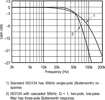 Figure 11. Gain vs. Frequency
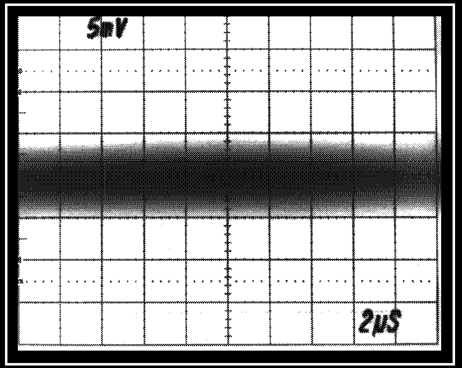 Figure 13. Filtered ISO124 (No Visible Output Ripple)
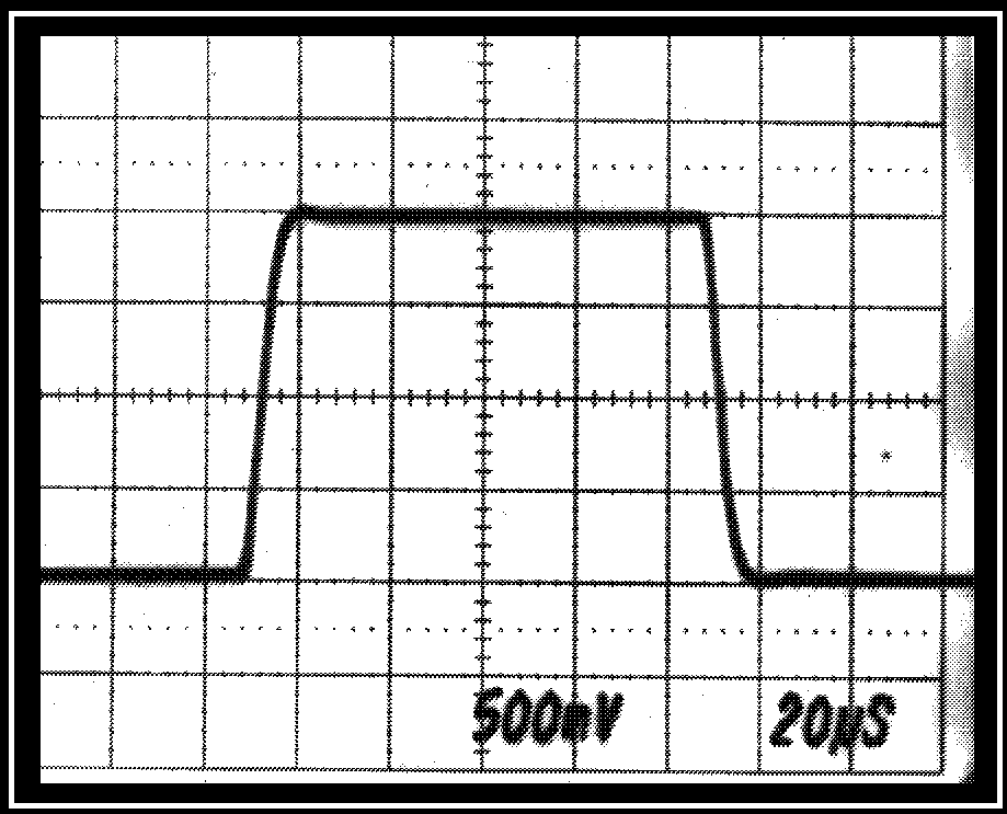 Figure 15. Step Response of ISO124 With Added Twopole Output Filter
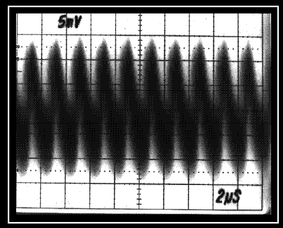
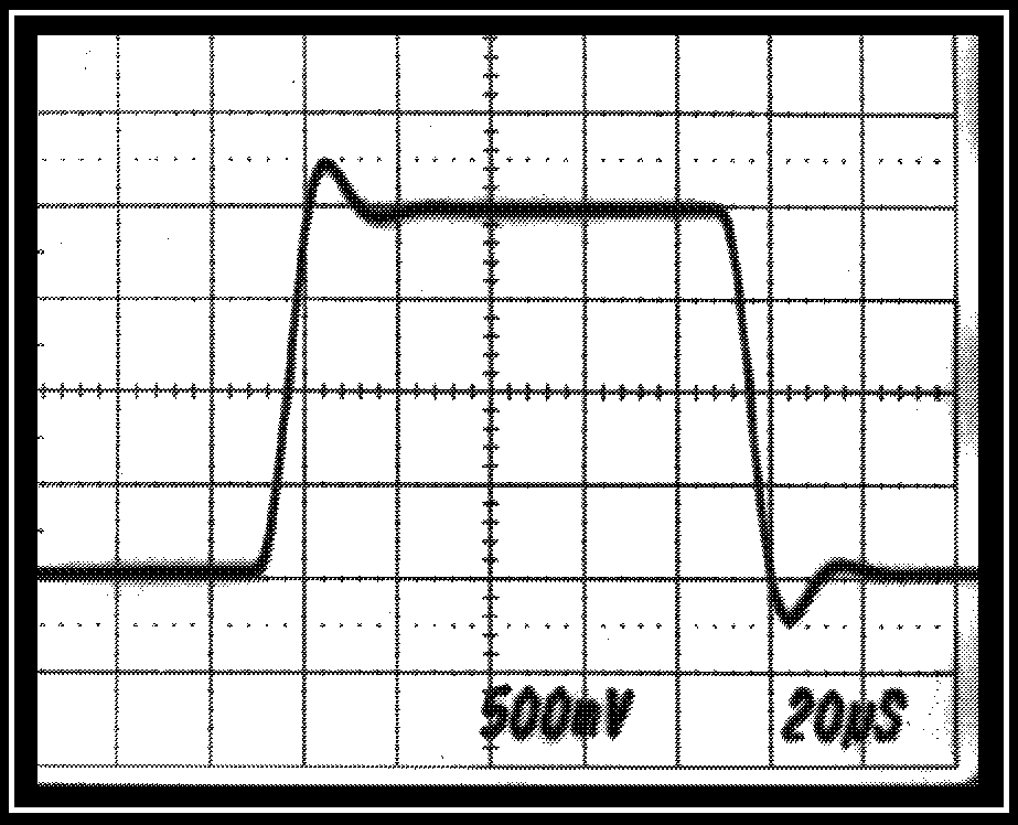 Figure 14. Step Response of Standard ISO124
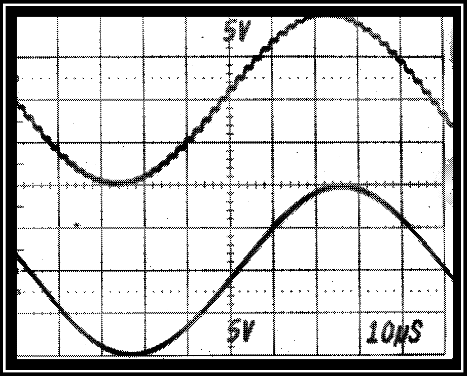 Figure 16. Large-signal, 10-kHz Sine-wave Response of ISO124 With and Without Output Filter