SLLSEW1 December 2016 ISO5852S-EP
PRODUCTION DATA.
- 1 Features
- 2 Applications
- 3 Description
- 4 Revision History
- 5 Description (continued)
- 6 Pin Configuration and Function
-
7 Specifications
- 7.1 Absolute Maximum Ratings
- 7.2 ESD Ratings
- 7.3 Recommended Operating Conditions
- 7.4 Thermal Information
- 7.5 Power Ratings
- 7.6 Insulation Specifications
- 7.7 Safety Limiting Values
- 7.8 Safety-Related Certifications
- 7.9 Electrical Characteristics
- 7.10 Switching Characteristics
- 7.11 Insulation Characteristics Curves
- 7.12 Typical Characteristics
- 8 Parameter Measurement Information
- 9 Detailed Description
-
10Application and Implementation
- 10.1 Application Information
- 10.2
Typical Applications
- 10.2.1 Design Requirements
- 10.2.2
Detailed Design Procedure
- 10.2.2.1 Recommended ISO5852S-EP Application Circuit
- 10.2.2.2 FLT and RDY Pin Circuitry
- 10.2.2.3 Driving the Control Inputs
- 10.2.2.4 Local Shutdown and Reset
- 10.2.2.5 Global-Shutdown and Reset
- 10.2.2.6 Auto-Reset
- 10.2.2.7 DESAT Pin Protection
- 10.2.2.8 DESAT Diode and DESAT Threshold
- 10.2.2.9 Determining the Maximum Available, Dynamic Output Power, POD-max
- 10.2.2.10 Example
- 10.2.2.11 Higher Output Current Using an External Current Buffer
- 10.2.3 Application Curves
- 11Power Supply Recommendations
- 12Layout
- 13Device and Documentation Support
- 14Mechanical, Packaging, and Orderable Information
Package Options
Mechanical Data (Package|Pins)
- DW|16
Thermal pad, mechanical data (Package|Pins)
- DW|16
Orderable Information
10 Application and Implementation
NOTE
Information in the following applications sections is not part of the TI component specification, and TI does not warrant its accuracy or completeness. TI’s customers are responsible for determining suitability of components for their purposes. Customers should validate and test their design implementation to confirm system functionality.
10.1 Application Information
The ISO5852S-EP device is an isolated gate driver for power semiconductor devices such as IGBTs and MOSFETs. It is intended for use in applications such as motor control, industrial inverters and switched mode power supplies. In these applications, sophisticated PWM control signals are required to turn the power devices on and off, which at the system level eventually may determine, for example, the speed, position, and torque of the motor or the output voltage, frequency and phase of the inverter. These control signals are usually the outputs of a microcontroller, and are at low voltage levels such as 2.5 V, 3.3 V or 5 V. The gate controls required by the MOSFETs and IGBTs, however, are in the range of 30-V (using unipolar output supply) to 15-V (using bipolar output supply), and require high-current capability to drive the large capacitive loads offered by those power transistors. The gate drive must also be applied with reference to the emitter of the IGBT (source for MOSFET), and by construction, the emitter node in a gate-drive system swings between 0 to the DC-bus voltage, which can be several 100s of volts in magnitude.
The ISO5852S-EP device is therefore used to level shift the incoming 2.5-V, 3.3-V, and 5-V control signals from the microcontroller to the 30-V (using unipolar output supply) to 15-V (using bipolar output supply) drive required by the power transistors while ensuring high-voltage isolation between the driver side and the microcontroller side.
10.2 Typical Applications
Figure 48 shows the typical application of a three-phase inverter using six ISO5852S-EP isolated gate drivers. Three-phase inverters are used for variable-frequency drives to control the operating speed of AC motors and for high-power applications such as high-voltage DC (HVDC) power transmission.
The basic three-phase inverter consists of three single-phase inverter switches each comprising two ISO5852S-EP devices that are connected to one of the three load terminals. The operation of the three switches is coordinated so that one switch operates at each 60 degree point of the fundamental output waveform, therefore creating a six-step line-to-line output waveform. In this type of applications, carrier-based PWM techniques are applied to retain waveform envelope and cancel harmonics.
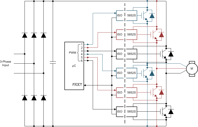 Figure 48. Typical Motor-Drive Application
10.2.1 Design Requirements
Unlike optocoupler-based gate drivers which required external current drivers and biasing circuitry to provide the input control signals, the input control to the ISO5852S-EP device is CMOS and can be directly driven by the microcontroller. Other design requirements include decoupling capacitors on the input and output supplies, a pullup resistor on the common-drain FLT output signal, and a high-voltage protection diode between the IGBT collector and the DESAT input. Additional details are explained in the subsequent sections. Table 2 lists the allowed range for input and output supply voltage, and the typical current output available from the gate-driver.
Table 2. Design Parameters
| PARAMETER | VALUE |
|---|---|
| Input supply voltage | 2.25 V to 5.5 V |
| Unipolar output-supply voltage (VCC2 – GND2 = VCC2 – VEE2) | 15 V to 30 V |
| Bipolar output-supply voltage (VCC2 – VEE2) | 15 V to 30 V |
| Bipolar output-supply voltage (GND2 – VEE2) | 0 V to 15 V |
| Output current | 2.5 A |
10.2.2 Detailed Design Procedure
10.2.2.1 Recommended ISO5852S-EP Application Circuit
The ISO5852S-EP device has both, inverting and noninverting gate-control inputs, an active-low reset input, and an open-drain fault output suitable for wired-OR applications. The recommended application circuit in Figure 49 shows a typical gate-driver implementation with unipolar output supply. Figure 50 shows a typical gate-driver implementation with bipolar output supply using the ISO5852S-EP device.
A 0.1-μF bypass capacitor, recommended at the VCC1 input supply pin, and 1-μF bypass capacitor, recommended at the VCC2 output supply pin, provide the large transient currents required during a switching transition to ensure reliable operation. The 220-pF blanking capacitor disables DESAT detection during the off-to-on transition of the power device. The DESAT diode (DDST) and the 1-kΩ series resistor on the DESAT pin are external protection components. The RG gate resistor limits the gate-charge current and indirectly controls the rise and fall times of the IGBT collector voltage. The open-drain FLT output and RDY output have a passive 10-kΩ pullup resistor. In this application, the IGBT gate driver is disabled when a fault is detected and does not resume switching until the microcontroller applies a reset signal.
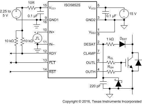 Figure 49. Unipolar Output Supply
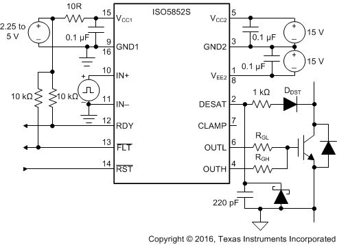 Figure 50. Bipolar Output Supply
10.2.2.2 FLT and RDY Pin Circuitry
A is 50-kΩ pullup resistor exists internally on FLT and RDY pins. The FLT and RDY pins are an open-drain output. A 10-kΩ pullup resistor can be used to make it faster rise and to provide logic high when FLT and RDY is inactive, as shown in Figure 51.
Fast common-mode transients can inject noise and glitches on FLT and RDY pins because of parasitic coupling. The injection of noise and glitches is dependent on board layout. If required, additional capacitance (100 pF to 300 pF) can be included on the FLT and RDY pins.
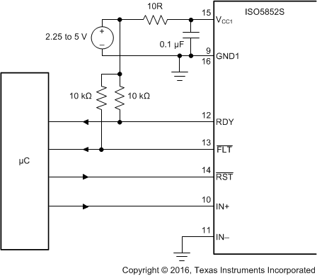 Figure 51. FLT and RDY Pin Circuitry for High CMTI
10.2.2.3 Driving the Control Inputs
The amount of common-mode transient immunity (CMTI) can be curtailed by the capacitive coupling from the high-voltage output circuit to the low-voltage input side of the ISO5852S-EP device. For maximum CMTI performance, the digital control inputs, IN+ and IN–, must be actively driven by standard CMOS, push-pull drive circuits. This type of low-impedance signal source provides active drive signals that prevent unwanted switching of the ISO5852S-EP output under extreme common-mode transient conditions. Passive drive circuits, such as open-drain configurations using pullup resistors, must be avoided. A 20-ns glitch filter exists that can filter a glitch up to 20 ns on IN+ or IN–.
10.2.2.4 Local Shutdown and Reset
In applications with local shutdown and reset, the FLT output of each gate driver is polled separately, and the individual reset lines are independently asserted low to reset the motor controller after a fault condition.
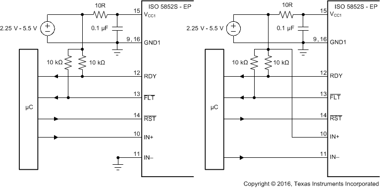 Figure 52. Local Shutdown and Reset for Noninverting (left) and Inverting Input Configuration (right)
10.2.2.5 Global-Shutdown and Reset
When configured for inverting operation, the ISO5852S-EP device can be configured to shutdown automatically in the event of a fault condition by tying the FLT output to IN+. For high reliability drives, the open drain FLT outputs of multiple ISO5852S-EP devices can be wired together forming a single, common fault bus for interfacing directly to the microcontroller. When any of the six gate drivers of a three-phase inverter detects a fault, the active-low FLT output disables all six gate drivers simultaneously.
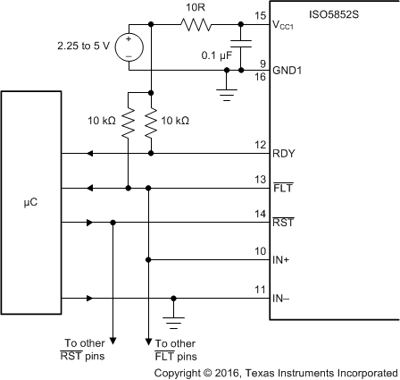 Figure 53. Global Shutdown With Inverting Input Configuration
10.2.2.6 Auto-Reset
In this case, the gate control signal at IN+ is also applied to the RST input to reset the fault latch every switching cycle. Incorrect RST makes output go low. A fault condition, however, the gate driver remains in the latched fault state until the gate control signal changes to the gate-low state and resets the fault latch.
If the gate control signal is a continuous PWM signal, the fault latch is always reset before IN+ goes high again. This configuration protects the IGBT on a cycle-by-cycle basis and automatically resets before the next on cycle.
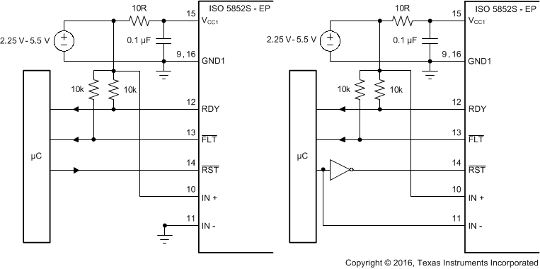 Figure 54. Auto Reset for Noninverting and Inverting Input Configuration
10.2.2.7 DESAT Pin Protection
Switching inductive loads causes large, instantaneous forward-voltage transients across the freewheeling diodes of the IGBTs. These transients result in large negative-voltage spikes on the DESAT pin which draw substantial current out of the device. To limit this current below damaging levels, a 100-Ω to 1-kΩ resistor is connected in series with the DESAT diode.
Further protection is possible through an optional Schottky diode, whose low-forward voltage assures clamping of the DESAT input to GND2 potential at low-voltage levels.
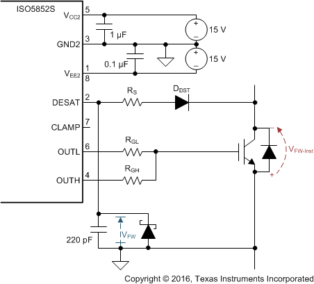 Figure 55. DESAT Pin Protection With Series Resistor and Schottky Diode
10.2.2.8 DESAT Diode and DESAT Threshold
The function of the DESAT diode is to conduct forward current, allowing sensing of the saturated collector-to-emitter voltage of the IGBT, V(DESAT), (when the IGBT is on), and to block high voltages (when the IGBT is off). During the short transition time when the IGBT is switching, a commonly high dVCE/dt voltage ramp rate occurs across the IGBT. This ramp rate results in a charging current I(CHARGE) = C(D-DESAT) × dVCE/dt, charging the blanking capacitor. C(D-DESAT) is the diode capacitance at DESAT.
To minimize this current and avoid false DESAT triggering, fast switching diodes with low capacitance are recommended. As the diode capacitance builds a voltage divider with the blanking capacitor, large collector voltage transients appear at DESAT attenuated by the ratio of 1+ C(BLANK) / C(D-DESAT).
Because the sum of the DESAT diode forward-voltage and the IGBT collector-emitter voltage make up the voltage at the DESAT-pin, VF + VCE = V(DESAT), the VCE level, which triggers a fault condition, can be modified by adding multiple DESAT diodes in series: VCE-FAULT(TH) = 9 V – n × VF (where n is the number of DESAT diodes).
When using two diodes instead of one, diodes with half the required maximum reverse-voltage rating can be selected.
10.2.2.9 Determining the Maximum Available, Dynamic Output Power, POD-max
The ISO5852S-EP maximum-allowed total power consumption of PD = 251 mW consists of the total input power, PID, the total output power, POD, and the output power under load, POL:
With:
and:
then:
In comparison to POL, the actual dynamic output power under worst case condition, POL-WC, depends on a variety of parameters:

where
- fINP = signal frequency at the control input IN+
- QG = power device gate charge
- VCC2 = positive output supply with respect to GND2
- VEE2 = negative output supply with respect to GND2
- ron-max = worst case output resistance in the on-state: 4 Ω
- roff-max = worst case output resistance in the off-state: 2.5 Ω
- RG = gate resistor
When RG is determined, Equation 5 is to be used to verify whether POL-WC < POL. Figure 56 shows a simplified output stage model for calculating POL-WC.
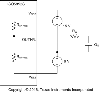 Figure 56. Simplified Output Model for Calculating POL-WC
10.2.2.10 Example
This examples considers an IGBT drive with the following parameters:
- ION-PK = 2 A
- QG = 650 nC
- fINP = 20 kHz
- VCC2 = 15 V
- VEE2 = –8 V
Applying the value of the gate resistor RG = 10 Ω.
Then, calculating the worst-case output-power consumption as a function of RG, using Equation 5 ron-max = worst case output resistance in the on-state: 4 Ω, roff-max = worst case output resistance in the off-state: 2.5 Ω, RG = gate resistor yields

Because POL-WC = 72.61 mW is less than the calculated maximum of POL = 88.25 mW, the resistor value of RG = 10 Ω is suitable for this application.
10.2.2.11 Higher Output Current Using an External Current Buffer
To increase the IGBT gate drive current, a non-inverting current buffer (such as the npn/pnp buffer shown in Figure 57) can be used. Inverting types are not compatible with the desaturation fault protection circuitry and must be avoided. The MJD44H11/MJD45H11 pair is appropriate for currents up to 8 A, the D44VH10/ D45VH10 pair for up to 15 A maximum.
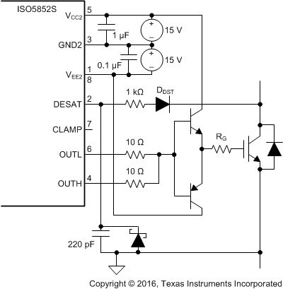 Figure 57. Current Buffer for Increased Drive Current
10.2.3 Application Curves
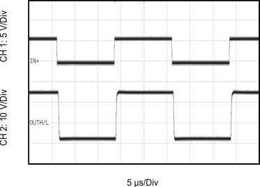
| CL = 1 nF | RGH = 10 Ω | RGL = 10 Ω |
| VCC2 – GND2 = 15 V | GND2 - VEE2 = 8 V | |
| (VCC2 – VEE2 = 23 V) |
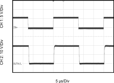
| CL = 1 nF | RGH = 10 Ω | RGL = 10 Ω |
| VCC2 – VEE2 = VCC2 - GND2 = 20 V | ||