SLLSEK8C January   2015  – April 2015 ISO7320C , ISO7320FC , ISO7321C , ISO7321FC

PRODUCTION DATA.  

  1. Features
  2. Applications
  3. Description
  4. Revision History
  5. Pin Configuration and Functions
  6. Specifications
    1. 6.1 Absolute Maximum Ratings
    2. 6.2 ESD Ratings
    3. 6.3 Recommended Operating Conditions
    4. 6.4 Thermal Information
    5. 6.5 Electrical Characteristics, 5 V
    6. 6.6 Electrical Characteristics, 3.3 V
    7. 6.7 Switching Characteristics, 5 V
    8. 6.8 Switching Characteristics, 3.3 V
    9. 6.9 Typical Characteristics
  7. Parameter Measurement Information
  8. Detailed Description
    1. 8.1 Overview
    2. 8.2 Functional Block Diagram
    3. 8.3 Feature Description
      1. 8.3.1 High Voltage Feature Description
        1. 8.3.1.1 Insulation and Safety-Related Specifications for D-8 Package
        2. 8.3.1.2 Insulation Characteristics
        3. 8.3.1.3 Regulatory Information
        4. 8.3.1.4 Safety Limiting Values
    4. 8.4 Device Functional Modes
      1. 8.4.1 Device I/O Schematics
  9. Applications and Implementation
    1. 9.1 Application Information
    2. 9.2 Typical Application
      1. 9.2.1 Design Requirements
        1. 9.2.1.1 Typical Supply Current Equations
      2. 9.2.2 Detailed Design Procedure
        1. 9.2.2.1 Electromagnetic Compatibility (EMC) Considerations
      3. 9.2.3 Application Performance Curves
  10. 10Power Supply Recommendations
  11. 11Layout
    1. 11.1 PCB Material
    2. 11.2 Layout Guidelines
    3. 11.3 Layout Example
  12. 12Device and Documentation Support
    1. 12.1 Related Links
    2. 12.2 Trademarks
    3. 12.3 Electrostatic Discharge Caution
    4. 12.4 Glossary
  13. 13Mechanical, Packaging, and Orderable Information

Package Options

Refer to the PDF data sheet for device specific package drawings

Mechanical Data (Package|Pins)
  • D|8
Thermal pad, mechanical data (Package|Pins)
Orderable Information

5 Pin Configuration and Functions

ISO7320
D PACKAGE
(TOP VIEW)
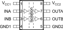
ISO7320C ISO7320FC ISO7321C ISO7321FC po_iso7320C_sllsek8.gif
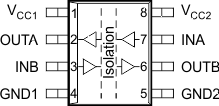
ISO7321
D PACKAGE
(TOP VIEW)
ISO7320C ISO7320FC ISO7321C ISO7321FC po_iso7321C_sllsek8.gif

Pin Functions

PIN I/O DESCRIPTION
NAME ISO7320 ISO7321
INA 2 7 I Input, channel A
INB 3 3 I Input, channel B
GND1 4 4 Ground connection for VCC1
GND2 5 5 Ground connection for VCC2
OUTA 7 2 O Output, channel A
OUTB 6 6 O Output, channel B
VCC1 1 1 Power supply, VCC1
VCC2 8 8 Power supply, VCC2