SLLSEC3F September 2012 – April 2016 ISO7631FC , ISO7631FM , ISO7641FC
PRODUCTION DATA.
- 1 Features
- 2 Applications
- 3 Description
- 4 Revision History
- 5 Pin Configuration and Functions
-
6 Specifications
- 6.1 Absolute Maximum Ratings
- 6.2 ESD Ratings
- 6.3 Recommended Operating Conditions
- 6.4 Thermal Information
- 6.5 Electrical Characteristics: VCC1 and VCC2 at 5 V ± 10%
- 6.6 Electrical Characteristics: VCC1 at 5 V ± 10% and VCC2 at 3.3 V ± 10%
- 6.7 Electrical Characteristics: VCC1 at 3.3 V ± 10% and VCC2 at 5 V ± 10%
- 6.8 Electrical Characteristics: VCC1 and VCC2 at 3.3 V ± 10%
- 6.9 Electrical Characteristics: VCC1 and VCC2 at 2.7 V (ISO7631FM Only)
- 6.10 Power Dissipation Characteristics
- 6.11 Supply Current Characteristics: VCC1 and VCC2 at 5 V ± 10%
- 6.12 Supply Current Characteristics: VCC1 at 5 V ± 10% and VCC2 at 3.3 V ± 10%
- 6.13 Supply Current Characteristics: VCC1 at 3.3 V ± 10% and VCC2 at 5 V ± 10%
- 6.14 Supply Current Characteristics: VCC1 and VCC2 at 3.3 V ± 10%
- 6.15 Supply Current Characteristics: VCC1 and VCC2 at 2.7 V (ISO7631FM Only) Only M-Grade devices are recommended for operation down to 2.7 V supplies. For 2.7 V-operation, max data rate is 100 Mbps.
- 6.16 Switching Characteristics: VCC1 and VCC2 at 5 V ± 10%
- 6.17 Switching Characteristics: VCC1 at 5 V ± 10% and VCC2 at 3.3 V ± 10%
- 6.18 Switching Characteristics: VCC1 at 3.3 V ± 10% and VCC2 at 5 V ± 10%
- 6.19 Switching Characteristics: VCC1 and VCC2 at 3.3 V ± 10%
- 6.20 Switching Characteristics: VCC1 and VCC2 at 2.7 V Only M-Grade devices are recommended for operation down to 2.7 V supplies. For 2.7 V-operation, max data rate is 100 Mbps.
- 6.21 Typical Characteristics
- 7 Parameter Measurement Information
- 8 Detailed Description
- 9 Application and Implementation
- 10Power Supply Recommendations
- 11Layout
- 12Device and Documentation Support
- 13Mechanical, Packaging, and Orderable Information
Package Options
Refer to the PDF data sheet for device specific package drawings
Mechanical Data (Package|Pins)
- DW|16
Thermal pad, mechanical data (Package|Pins)
Orderable Information
9 Application and Implementation
NOTE
Information in the following applications sections is not part of the TI component specification, and TI does not warrant its accuracy or completeness. TI’s customers are responsible for determining suitability of components for their purposes. Customers should validate and test their design implementation to confirm system functionality.
9.1 Application Information
ISO7641FC uses single-ended TTL-logic switching technology. It has a supply voltage range from 3 V to 5.5 V for both supplies, VCC1 and VCC2. When designing with digital isolators, it is important to note that due to the single-ended design structure, digital isolators do not conform to any specific interface standard and are only intended for isolating single-ended CMOS or TTL digital signal lines. The isolator is typically placed between the data controller (that is, μC or UART), and a data converter or a line transceiver, regardless of the interface type or standard.
9.2 Typical Application
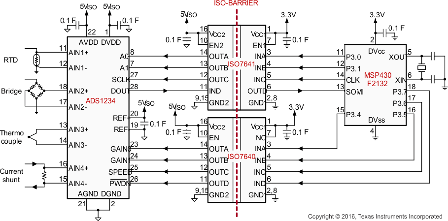 Figure 24. Isolated Data Acquisition System for Process Control
9.2.1 Design Requirements
Unlike optocouplers, which require external components to improve performance, provide bias, or limit current, the ISO76xx device only requires two external bypass capacitors to operate.
9.2.2 Detailed Design Procedure
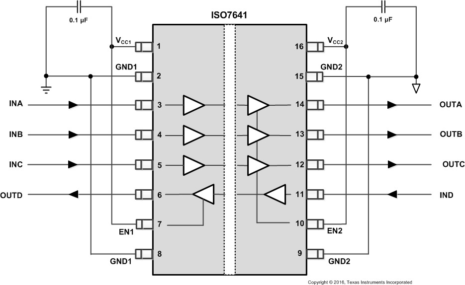 Figure 25. Typical ISO7641FC Circuit Hookup
Typical Supply Current Equations
(Calculated based on room temperature and typical Silicon process)ISO7631FM:
At VCC1 = VCC2 = 3.3 V
At VCC1 = VCC2 = 5 V
ISO7631FC:
At VCC1 = VCC2 = 3.3 V
At VCC1 = VCC2 = 5 V
ISO7641FC:
At VCC1 = VCC2 = 3.3 V
At VCC1 = VCC2 = 5 V
ICC1 and ICC2 are typical supply currents measured in mA; f is data rate measured in Mbps; CL is the capacitive load on each channel measured in pF.
9.2.3 Application Curves
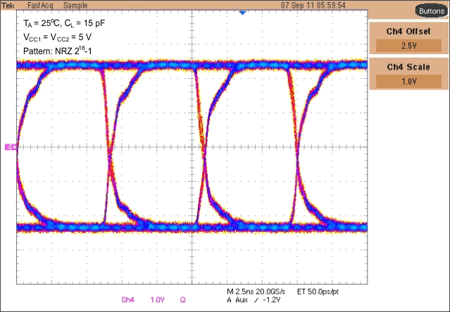 Figure 26. M-Grade Typical Eye Diagram at 150 Mbps,
 5 V Operation
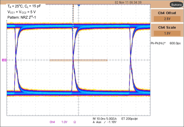 Figure 28. C-Grade Typical Eye Diagram at 25 Mbps, 5 V Operation
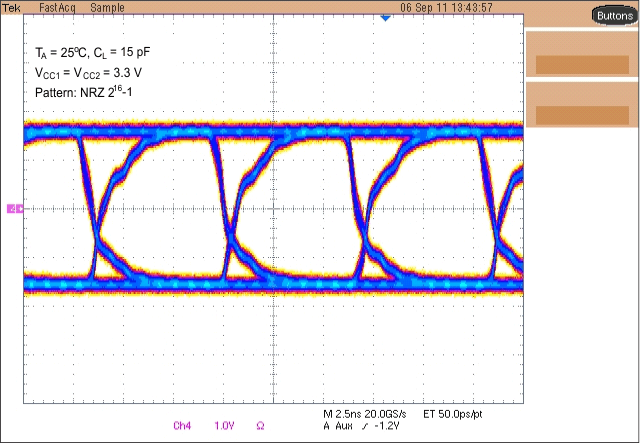 Figure 27. M-Grade Typical Eye Diagram at 150 Mbps,
 3.3 V Operation
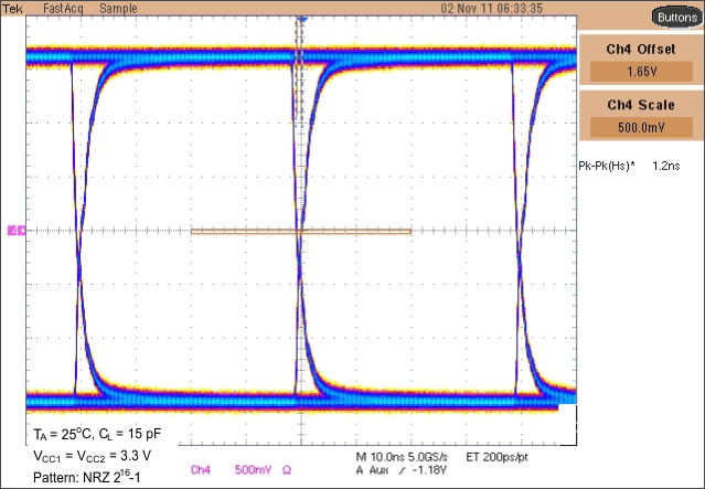 Figure 29. C-Grade Typical Eye Diagram at 25 Mbps, 3.3 V Operation