SLLSEC3F September 2012 – April 2016 ISO7631FC , ISO7631FM , ISO7641FC
PRODUCTION DATA.
- 1 Features
- 2 Applications
- 3 Description
- 4 Revision History
- 5 Pin Configuration and Functions
-
6 Specifications
- 6.1 Absolute Maximum Ratings
- 6.2 ESD Ratings
- 6.3 Recommended Operating Conditions
- 6.4 Thermal Information
- 6.5 Electrical Characteristics: VCC1 and VCC2 at 5 V ± 10%
- 6.6 Electrical Characteristics: VCC1 at 5 V ± 10% and VCC2 at 3.3 V ± 10%
- 6.7 Electrical Characteristics: VCC1 at 3.3 V ± 10% and VCC2 at 5 V ± 10%
- 6.8 Electrical Characteristics: VCC1 and VCC2 at 3.3 V ± 10%
- 6.9 Electrical Characteristics: VCC1 and VCC2 at 2.7 V (ISO7631FM Only)
- 6.10 Power Dissipation Characteristics
- 6.11 Supply Current Characteristics: VCC1 and VCC2 at 5 V ± 10%
- 6.12 Supply Current Characteristics: VCC1 at 5 V ± 10% and VCC2 at 3.3 V ± 10%
- 6.13 Supply Current Characteristics: VCC1 at 3.3 V ± 10% and VCC2 at 5 V ± 10%
- 6.14 Supply Current Characteristics: VCC1 and VCC2 at 3.3 V ± 10%
- 6.15 Supply Current Characteristics: VCC1 and VCC2 at 2.7 V (ISO7631FM Only) Only M-Grade devices are recommended for operation down to 2.7 V supplies. For 2.7 V-operation, max data rate is 100 Mbps.
- 6.16 Switching Characteristics: VCC1 and VCC2 at 5 V ± 10%
- 6.17 Switching Characteristics: VCC1 at 5 V ± 10% and VCC2 at 3.3 V ± 10%
- 6.18 Switching Characteristics: VCC1 at 3.3 V ± 10% and VCC2 at 5 V ± 10%
- 6.19 Switching Characteristics: VCC1 and VCC2 at 3.3 V ± 10%
- 6.20 Switching Characteristics: VCC1 and VCC2 at 2.7 V Only M-Grade devices are recommended for operation down to 2.7 V supplies. For 2.7 V-operation, max data rate is 100 Mbps.
- 6.21 Typical Characteristics
- 7 Parameter Measurement Information
- 8 Detailed Description
- 9 Application and Implementation
- 10Power Supply Recommendations
- 11Layout
- 12Device and Documentation Support
- 13Mechanical, Packaging, and Orderable Information
Package Options
Refer to the PDF data sheet for device specific package drawings
Mechanical Data (Package|Pins)
- DW|16
Thermal pad, mechanical data (Package|Pins)
Orderable Information
11 Layout
11.1 Layout Guidelines
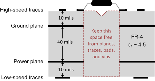
A minimum of four layers is required to accomplish a low EMI PCB design (see Figure 30). Layer stacking should be in the following order (top-to-bottom): high-speed signal layer, ground plane, power plane and low-frequency signal layer.
- Routing the high-speed traces on the top layer avoids the use of vias (and the introduction of their inductances) and allows for clean interconnects between the isolator and the transmitter and receiver circuits of the data link.
- Placing a solid ground plane next to the high-speed signal layer establishes controlled impedance for transmission line interconnects and provides an excellent low-inductance path for the return current flow.
- Placing the power plane next to the ground plane creates additional high-frequency bypass capacitance of approximately 100 pF/in2.
- Routing the slower speed control signals on the bottom layer allows for greater flexibility as these signal links usually have margin to tolerate discontinuities such as vias.
If an additional supply voltage plane or signal layer is needed, add a second power and ground plane system to the stack to keep it symmetrical. This makes the stack mechanically stable and prevents it from warping. Also the power and ground plane of each power system can be placed closer together, thus increasing the high-frequency bypass capacitance significantly.
NOTE
For detailed layout recommendations, see Digital Isolator Design Guide, SLLA284.
11.2 Layout Example
 Figure 30. Recommended Layer Stack