SLLSFW6 March 2024 ISOUSB211-Q1
ADVANCE INFORMATION
- 1
- 1 Features
- 2 Applications
- 3 Description
- 4 Pin Configuration and Functions
-
5 Specifications
- 5.1 Absolute Maximum Ratings
- 5.2 ESD Ratings
- 5.3 Recommended Operating Conditions
- 5.4 Thermal Information
- 5.5 Power Ratings
- 5.6 Insulation Specifications
- 5.7 Safety-Related Certifications
- 5.8 Safety Limiting Values
- 5.9 Electrical Characteristics
- 5.10 Switching Characteristics
- 5.11 Insulation Characteristics Curves
- 5.12 Typical Characteristics
- 6 Parameter Measurement Information
-
7 Detailed Description
- 7.1 Overview
- 7.2 Functional Block Diagram
- 7.3
Feature Description
- 7.3.1 Power Supply Options
- 7.3.2 Power Up
- 7.3.3 Symmetric Operation, Dual-Role Port and Role-Reversal
- 7.3.4 Connect and Speed Detection
- 7.3.5 Disconnect Detection
- 7.3.6 Reset
- 7.3.7 LS/FS Message Traffic
- 7.3.8 HS Message Traffic
- 7.3.9 Equalization and Pre-emphasis
- 7.3.10 L2 Power Management State (Suspend) and Resume
- 7.3.11 L1 Power Management State (Sleep) and Resume
- 7.3.12 HS Test Mode Support
- 7.3.13 CDP Advertising
- 7.4 Device Functional Modes
- 8 Application and Implementation
- 9 Device and Documentation Support
- 10Revision History
- 11Mechanical, Packaging, and Orderable Information
Package Options
Mechanical Data (Package|Pins)
- DP|28
Thermal pad, mechanical data (Package|Pins)
Orderable Information
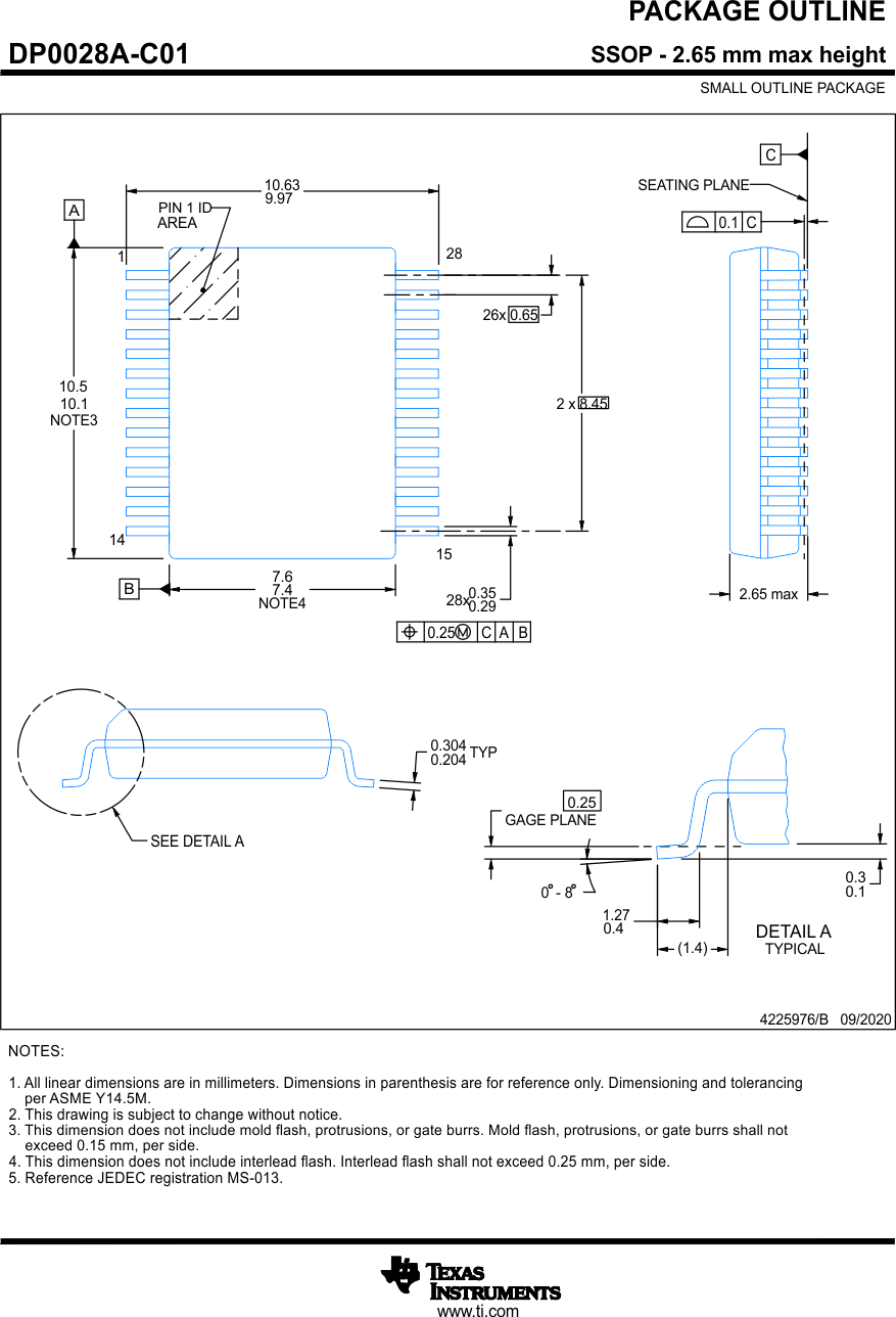
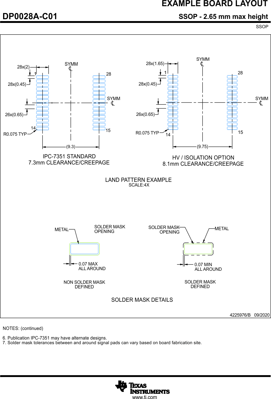
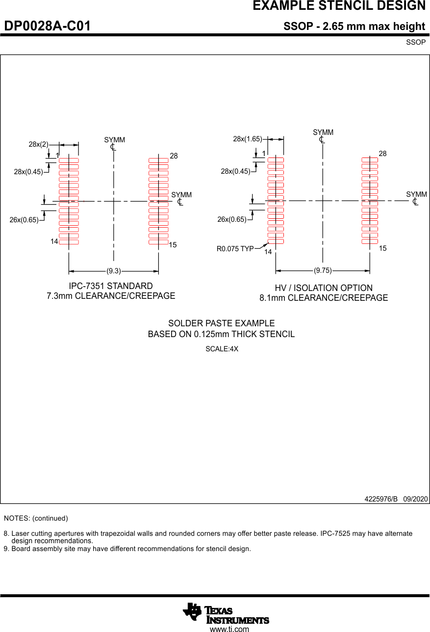
11 Mechanical, Packaging, and Orderable Information
The following pages include mechanical packaging and orderable information. This information is the most current data available for the designated devices. This data is subject to change without notice and revision of this document. For browser-based versions of this data sheet, refer to the left-hand navigation.