SWRS313 July   2023 IWRL1432

ADVANCE INFORMATION  

  1.   1
  2. Features
  3. Applications
  4. Description
  5. Functional Block Diagram
  6. Revision History
  7. Device Comparison
    1. 6.1 Related Products
  8. Terminal Configurations and Functions
    1. 7.1 Pin Diagrams
    2. 7.2 Signal Descriptions
      1.      12
      2.      13
      3.      14
      4.      15
      5.      16
      6.      17
      7.      18
      8.      19
      9.      20
      10.      21
      11.      22
      12.      23
      13.      24
      14.      25
      15.      26
      16.      27
      17.      28
    3.     29
  9. Specifications
    1. 8.1  Absolute Maximum Ratings
    2. 8.2  ESD Ratings
    3. 8.3  Power-On Hours (POH)
    4. 8.4  Recommended Operating Conditions
    5. 8.5  Power Supply Specifications
      1. 8.5.1 Power Optimized 3.3V I/O Topology
      2. 8.5.2 BOM Optimized 3.3V I/O Topology
      3. 8.5.3 Power Optimized 1.8V I/O Topology
      4. 8.5.4 BOM Optimized 1.8V I/O Topology
      5. 8.5.5 System Topologies
        1. 8.5.5.1 Power Topologies
          1. 8.5.5.1.1 BOM Optimized Mode
          2. 8.5.5.1.2 Power Optimized Mode
      6. 8.5.6 Noise and Ripple Specifications
    6. 8.6  Power Save Modes
      1. 8.6.1 Typical Power Consumption Numbers
    7. 8.7  Peak Current Requirement per Voltage Rail
    8. 8.8  RF Specification
    9. 8.9  Supported DFE Features
    10. 8.10 CPU Specifications
    11. 8.11 Thermal Resistance Characteristics
    12. 8.12 Timing and Switching Characteristics
      1. 8.12.1  Power Supply Sequencing and Reset Timing
      2. 8.12.2  Synchronized Frame Triggering
      3. 8.12.3  Input Clocks and Oscillators
        1. 8.12.3.1 Clock Specifications
      4. 8.12.4  MultiChannel buffered / Standard Serial Peripheral Interface (McSPI)
        1. 8.12.4.1 McSPI Features
        2. 8.12.4.2 SPI Timing Conditions
        3. 8.12.4.3 SPI—Controller Mode
          1. 8.12.4.3.1 Timing and Switching Requirements for SPI - Controller Mode
          2. 8.12.4.3.2 Timing and Switching Characteristics for SPI Output Timings—Controller Mode
        4. 8.12.4.4 SPI—Peripheral Mode
          1. 8.12.4.4.1 Timing and Switching Requirements for SPI - Peripheral Mode
          2. 8.12.4.4.2 Timing and Switching Characteristics for SPI Output Timings—Secondary Mode
      5. 8.12.5  RDIF Interface Configuration
        1. 8.12.5.1 RDIF Interface Timings
        2. 8.12.5.2 RDIF Data Format
      6. 8.12.6  General-Purpose Input/Output
        1. 8.12.6.1 Switching Characteristics for Output Timing versus Load Capacitance (CL)
      7. 8.12.7  Controller Area Network - Flexible Data-rate (CAN-FD)
        1. 8.12.7.1 Dynamic Characteristics for the CANx TX and RX Pins
      8. 8.12.8  Serial Communication Interface (SCI)
        1. 8.12.8.1 SCI Timing Requirements
      9. 8.12.9  Inter-Integrated Circuit Interface (I2C)
        1. 8.12.9.1 I2C Timing Requirements
      10. 8.12.10 Quad Serial Peripheral Interface (QSPI)
        1. 8.12.10.1 QSPI Timing Conditions
        2. 8.12.10.2 Timing Requirements for QSPI Input (Read) Timings
        3. 8.12.10.3 QSPI Switching Characteristics
      11. 8.12.11 JTAG Interface
        1. 8.12.11.1 JTAG Timing Conditions
        2. 8.12.11.2 Timing Requirements for IEEE 1149.1 JTAG
        3. 8.12.11.3 Switching Characteristics Over Recommended Operating Conditions for IEEE 1149.1 JTAG
  10. Detailed Description
    1. 9.1 Overview
    2. 9.2 Functional Block Diagram
    3. 9.3 Subsystems
      1. 9.3.1 RF and Analog Subsystem
      2. 9.3.2 Clock Subsystem
      3. 9.3.3 Transmit Subsystem
      4. 9.3.4 Receive Subsystem
      5. 9.3.5 Processor Subsystem
      6. 9.3.6 Host Interface
      7. 9.3.7 Main Subsystem Cortex-M4F
      8. 9.3.8 Hardware Accelerator (HWA1.2) Features
        1. 9.3.8.1 Hardware Accelerator Feature Differences Between HWA1.1 and HWA1.2
    4. 9.4 Other Subsystems
      1. 9.4.1 GPADC Channels (Service) for User Application
      2. 9.4.2 GPADC Parameters
    5. 9.5 Memory Partitioning Options
    6. 9.6 Boot Modes
  11. 10Applications, Implementation, and Layout
    1. 10.1 Application Information
    2. 10.2 Reference Schematic
  12. 11Device and Documentation Support
    1. 11.1 Device Nomenclature
    2. 11.2 Tools and Software
    3. 11.3 Documentation Support
    4. 11.4 Support Resources
    5. 11.5 Trademarks
    6. 11.6 Electrostatic Discharge Caution
    7. 11.7 Glossary
  13. 12Mechanical, Packaging, and Orderable Information

Package Options

Mechanical Data (Package|Pins)
  • AMF|102
Thermal pad, mechanical data (Package|Pins)
Orderable Information

Clock Subsystem

The IWRL1432 clock subsystem generates 76 to 81 GHz from an input reference from a crystal. It has a built-in oscillator circuit followed by a clean-up PLL and a RF synthesizer circuit. The output of the RF synthesizer is then processed by an X4 multiplier to create the required frequency in the 76 to 81 GHz spectrum. The RF synthesizer output is modulated by the timing engine block to create the required waveforms for effective sensor operation.

The clean-up PLL also provides a reference clock for the host processor after system wakeup.

The clock subsystem also has built-in mechanisms for detecting the presence of a crystal and monitoring the quality of the generated clock.

Figure 9-2 describes the clock subsystem.
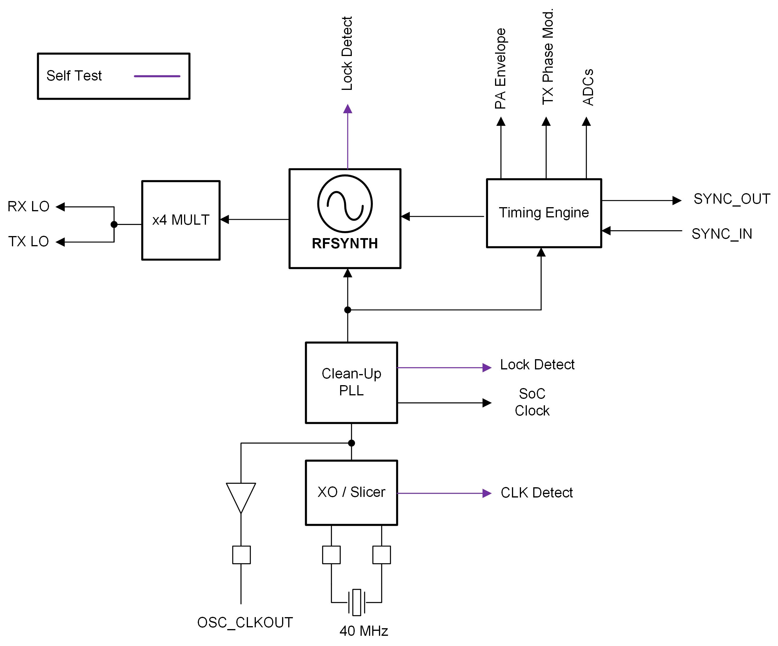
GUID-604522CB-9189-4DBD-9A8D-B4DA02DCC58B-low.jpg Figure 9-2 Clock Subsystem